A Method for Improving the Radiation Pattern of a Printed Sleeve Dipole Antenna Installed on a Portable Device
Abstract
Radiation patterns of an antenna with nearby metallic objects are distorted to a varying degree and in some cases a corrective measure may be necessary. In this paper we investigate the problem and solution of pattern distortion of a printed sleeve dipole antenna installed close to a printed circuit board of a portable communication device operating at 900-MHz band. First the pattern distortion of the dipole antenna caused by a printed circuit board of the portable device is analyzed using a commercial simulation tool. Then a method is proposed for improving the distorted antenna radiation pattern, which consists of a metal wire and a bent metal strip placed at the bottom of the printed circuit board. Optimum dimensions of a metal wire and a metal strip have been found from a parametric analysis. Finally it is shown that the proposed method restores the dipole's distorted radiation pattern nearly to the undistorted original form.
초록
근처에 금속물체가 있는 안테나의 방사패턴은 여러 정도로 왜곡이 되며 어떤 경우에는 이를 수정하기 위한 수단이 요구된다. 본 논문에서는 900-MHz 대역에서 동작하는 휴대용 통신장치의 인쇄회로 기판 가까이 설치된 인쇄형 슬리브 다이폴의 방사패턴 왜곡 문제와 해결책을 조사하였다. 우선 상용 시뮬레이션 툴을 사용하여 휴대장치의 인쇄회로 기판에 의해 초래된 다이폴 안테나의 방사패턴 왜곡을 분석하였다. 다음으로 왜곡된 안테나 방사패턴을 개선하기 위해 금속도선과 절곡된 금속 띠로 구성된 방법을 제안하였다. 변수해석 결과로부터 금속도선과 금속띠의 최적치수를 얻었다. 마지막으로 제안된 방법이 다이폴의 왜곡된 방사패턴을 거의 왜곡되지 않은 원래 형태로 복원함을 보였다.
Keywords:
dipole antenna, metallic objects, portable device, radiation pattern distortionI. Introduction
Antennas for portable communication devices are very important for commercial, government, and military applications and several previous works have been published on the subject [1]-[4]. The monopole antenna and its variants are widely used in portable devices due to the possibility of miniaturization and design flexibility such as external operation [5], internal operation (intenna) [6], wideband [7] or multiband capability [8], and MIMO configuration [9].
Though not as popular as the monopole antenna, the dipole antenna finds applications in portable devices [10]-[12]. The dipole antenna is more frequently used as an external unit to take advantage of the fact that the dipole does not require a ground plane. In using a dipole fed by a coaxial cable, an important issue is to suppress the current on a feeding coaxial cable which contributes to radiation pattern distortion and cross-polarized radiation [13].
Another important issue related to the dipole antenna on a portable device is the pattern distortion due to metal structures of the device such as printed circuit boards, brackets, enclosures, component shield cans, and device cases [14][15]. This issue has not received much attention in the antenna community, the reason of which is believed due to the fact that the problem needs to be solved for each specific case and a general solution is difficult to formulate.
In this paper, we propose a method for improving the radiation pattern of a printed sleeve dipole antenna installed on a portable device. The dipole's pattern is distorted by a printed circuit board (PCB) of the device and needs to be corrected for horizontally omnidirectional and vertically symmetric characteristics. It is shown that the PCB's pattern distortion effect can be corrected by optimally placing a bent parasitic metal strip connected to the bottom center of the PCB with a metal wire.
II. Dipole Pattern Improvement
2.1 Radiation Pattern of a Dipole Antenna
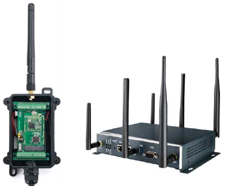
For LoRa communication [16], wire or printed dipoles encased in a plastic cylinder are popular as an external antenna as shown in Fig. 1 [17][18]. One can notice that the antenna length is comparable to the size of a device PCB or a device case. Metallic objects with a size greater than about a quarter wavelength incur both the impedance mismatch and pattern distortion to a varying degree.
In the first case depicted in Fig. 1, the device is under a dipole antenna, one can expect that the effect of a device PCB on the antenna characteristics is minimal since it is in the direction of the smallest antenna gain. In the second case, the antenna performance degradation can be more pronounced due to a horizontally placed metal case and due to the presence of other vertical antennas.
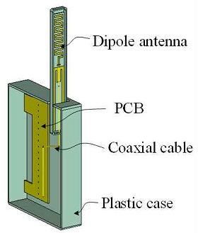
In this paper, we propose a method for improving the distorted radiation pattern of a printed sleeve dipole antenna installed beside a PCB with a partial overlap as shown in Fig. 2. The antenna operates at 850-940 MHz and a portable device can be a LoRa sensor node or a LoRa location tracker or a UHF short range radio terminal.
In Fig. 2, a dipole antenna is connected to the device's PCB via a coaxial cable. The dipole antenna is implemented in a printed form on a rigid and strong substrate material (FR-4) for strength and easy integration with the device chassis. The coaxial cable can be of flexible type so that the dipole antenna can be stowed away inside the case when the antenna is not in use and retracted when it is in use.
The device's case is made of plastic material (ABS with ϵr = 3.1 and tan δtan = 0.014). The dimensions (mm) of the device case are as follows: width = 101.5, height = 122.5, depth = 25.0, and wall thickness = 2.0. The PCB has a metal ground plane, signal traces, and electronic components. In antenna's point of view, the PCB can be treated as a uniform metal plate.
The presence of a PCB metal ground plane distorts the dipole's radiation pattern. For example, the azimuth symmetry of the pattern is destroyed and the peak gain angle is tilted downward from the horizon. The pattern distortion results in a non-omnidirectional performance and a reduced gain in the horizontal direction, which needs to be corrected or improved in some applications.
Starting with the radiation pattern of a dipole antenna alone, we will show the antenna pattern distorted by a PCB and then the pattern improved by the method proposed in this paper.
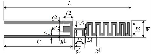
Fig. 3 shows the structure of the dipole antenna considered in this paper. The antenna consists of a meandered line for the dipole's upper arm, a sleeve for the dipole's lower arm, and a coaxial cable feeding the dipole antenna. The meandered line is used to reduce the length of the dipole upper arm. The sleeve is used for suppressing the radiation from the coaxial cable.
Fig. 4 shows the dimensional parameters of the sleeve dipole antenna. The antenna dimensions have been obtained for operation at around 900 MHz using a commercial electromagnetic-wave simulation tool (CST Studio Suite) and are shown in Table 1.
The coaxial cable feeding the antenna has the following parameters: center conductor diameter = 0.29 mm, inside/outside diameters of the outer conductor = 0.92/1.19 mm, and insulation material's dielectric constant and loss tangent = 2.1/0.0006. The dipole antenna is realized on a substrate with the following properties: dielectric constant = 4.3, loss tangent = 0.02, dielectric thickness = 1.0 mm, and metalization thickness = 0.035 mm.
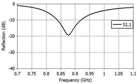
Characteristics of the dipole antenna have been simulated when the dipole antenna is alone in a free space. Fig. 5 shows the reflection coefficient of the dipole antenna with dimensions shown in Table 1. The reflection coefficient is less then -10 dB over 83 MHz around the center frequency 875 MHz (9.5% bandwidth).
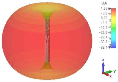
Fig. 6 shows the 3D absolute gain pattern of the dipole antenna alone. The gain pattern has an angular symmetry around the dipole axis. The maximum gain is 1.65 dBi.
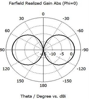
We have used a pattern analysis tool in CST Studio Suite for the accurate estimation of radiation pattern parameters. Fig. 7 shows the vertical gain pattern of the dipole antenna alone at ϕ = 0° and f = 915 MHz. The pattern is symmetric in the vertical direction. The maximum gain is 1.65 dBi occuring at θ = 90.8° with a 3-dB beamwidth of 82.6°.
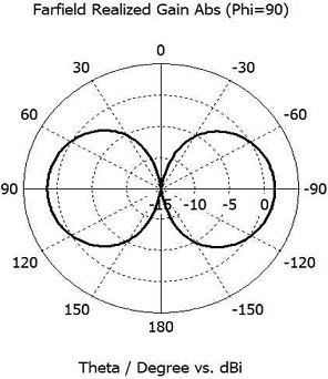
Fig. 8 shows the vertical gain pattern of the dipole antenna alone at ϕ = 90° and f = 915 MHz. The pattern is again symmetric in the vertical direction. The maximum gain is 1.61 dBi occurring at θ = 91.0° with a 3-dB beamwidth of 82.7°.
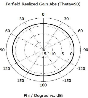
Fig. 9 shows the horizontal gain pattern (θ = 90°). The maximum gain is 1.65 dBi while the minimum is 1.61 dBi showing an excellent omnidirectional pattern.
2.2 Analysis of Radiation Pattern Distortion
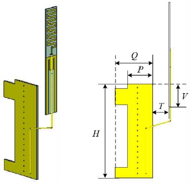
Next we will show the distortion of the dipole antenna's radiation pattern distortion caused by the presence of the PCB. Fig. 10 shows a simulation model and its dimensions. The plastic case of the device shown in Fig. 2 is omitted since it has little effect on the pattern distortion. The dimensions in mm of the simulation model are as follows: H = 105, Q = 45, P = 30, T = 20, and V = 25.5.
The structure and dimensions in Fig. 10 are just an example that we used for the illustration of the pattern improvement method proposed in this paper. Other metallic structures around the dipole antenna may require a different approach to the pattern improvement problem.
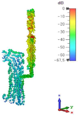
First, the current density on the dipole and the PCB surface have been simulated and shown in Fig. 11. The current density on the PCB is appreciable and flows in the same direction as the dipole current. The total current on the PCB is significant since the PCB surface area is much greater than the dipole strip area.
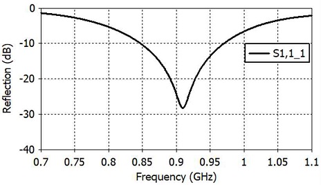
Fig. 12 shows the reflection coefficient of the dipole-PCB combined structure of Fig. 10. The reflection coefficient is less then -10 dB over 123 MHz around a center frequency 909 MHz (13.5% bandwidth). Compared with the case of the dipole alone, the center frequency is increased by 34 MHz and the bandwidth by 4%.
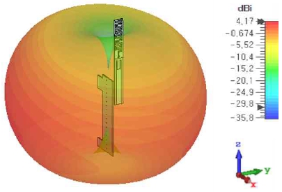
Fig. 13 shows the 3D absolute gain pattern of the structure shown in Fig. 10 along with the simulation model and the coordinate axes. In Fig. 13, one can see that the radiation pattern is distorted from an horizontally omnidirectional and vertically symmetric shape. The maximum gain is increased from 1.65 dBi of the dipole alone to 4.17 dBi. The maximum gain is in the direction of the PCB.
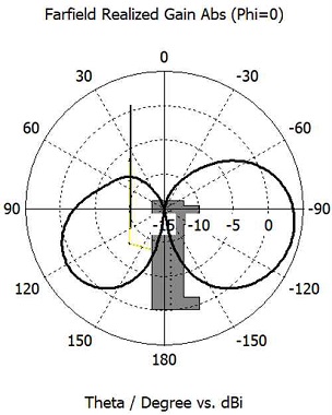
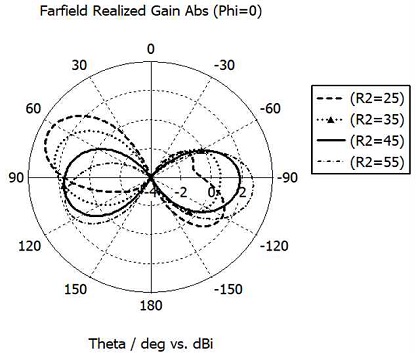
The pattern distortion can be seen more clearly in Figs. 14 and 15 which show elevation gain patterns in the zx-plane (ϕ = 0°, parallel to the PCB ground plane) and in the yz-plane (ϕ = 90°, perpendicular to the PCB ground plane) respectively. The pattern distortion is more pronounced in the plane parallel to the PCB ground plane.
We have used a pattern analysis tool in CST Studio Suite for the accurate estimation of the pattern distortion. At ϕ = 0°, the maximum gain is 1.51 dBi occurring at 32.5° below the horizon (θ = 122.5°) with a 3-dB beamwidth of 58.4°, while at ϕ = 180°, the maximum gain is 4.18 dBi occurring at θ = -101.0° with a beamwidth of 66.7°. The PCB ground plane directs more energy in the ϕ = 180° direction.
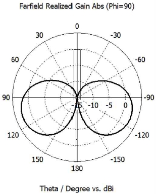
Fig. 15 shows the gain pattern in the ϕ = 90° plane. The gain pattern is symmetric with respect to the z axis due to a structural symmetry. At ϕ = 270°, the maximum gain is 1.82 dBi occurring at θ = -92.0 with a 3-dB beamwidth of 81.7°.
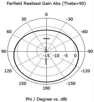
Fig. 16 shows the gain pattern in the xy-plane (θ = 90°). The maximum and minimum gains are 3.85 dBi at ϕ = 178.0° and -2.14 dBi at ϕ = 0.1° respectively. This is a significant deviation from a omnidirectional pattern of Fig. 9.
2.3 Improvement of Radiation Pattern
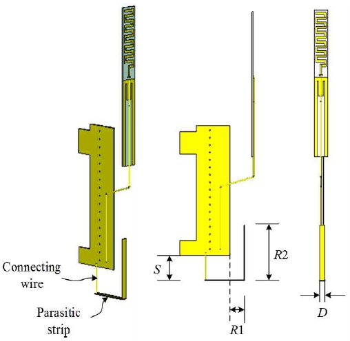
To correct the pattern distortion caused by the presence of a PCB, we employed a metal wire and a bent parasitic metal strip. The connecting wire is joined to the PCB at the PCB's bottom center edge as shown in Fig. 17. We have experimented with various parasitic metal strip geometries and found that the structure shown in Fig. 16 gives a good pattern symmetry.
Notice that the vertical portion of the parasitic strip is in the dipole's side with respect to the PCB. The connecting wire makes the PCB current flow onto the parasitic strip. Currents flowing on the connecting wire and parasitic strip enhance the antenna gain in the ϕ = 0° direction and moves the radiation pattern upward in the vertical plane so that the maximum gain occurs near the θ = 90° plane with a good symmetry around the z axis.
The dimensional parameters of the connecting wire and the parasitic strip are shown in Fig. 17. The optimum dimensions of the connecting wire and the parasitic strip have been obtained for the best pattern performance based on a parametric analysis. Their values in mm are: S = 20, R1 = 15, R2 = 45, and D = 5.
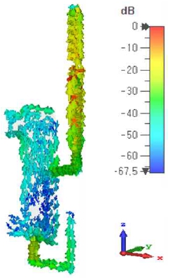
The surface current density on the proposed structure has been simulated and plotted in Fig. 18. A significant amount of the current flows on the connecting wire and on the parasitic strip.
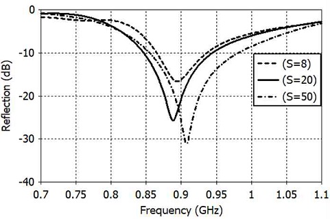
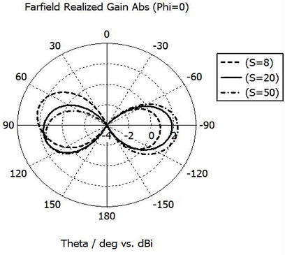
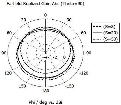
First we investigate the effect of the length S of the connecting wire with all the other dimensions fixed at their optimum values. Figs. 19-21 show the antenna's reflection coefficient and gain patterns when the connecting wire length S is 8, 20, and 50 mm.
The length of the connecting wire has a non-negligible effect on the reflection coefficient of the antenna as shown in Fig. 19. Good pattern symmetry in the vertical and horizontal planes can be obtained with a proper choice of S as we can see in Figs. 20 and 21. The optimum value of S is 20 mm.
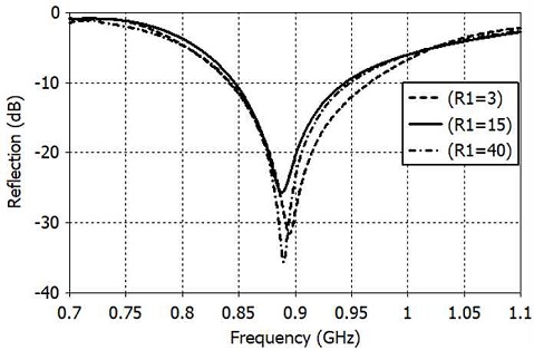
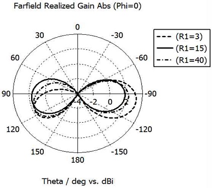
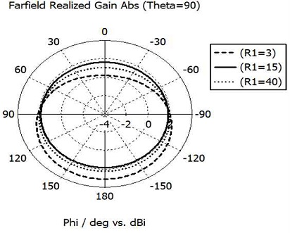
Next the effect of R1 in Fig. 17 (the position of the vertical portion of the parasitic strip) is investigated for R1 = 3, 15, and 40 mm. Fig. 22 shows the reflection coefficient versus R1, where one can see that the reflection coefficient is not sensitive to R1. Figs. 23 and 24 show the gain patterns at ϕ = 0° and at θ = 90° versus R1. We can see that there is an optimum value of R1 that gives a good pattern symmetry in the vertical and horizontal planes. The optimum value of R1 has been found to be 15 mm.
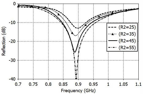
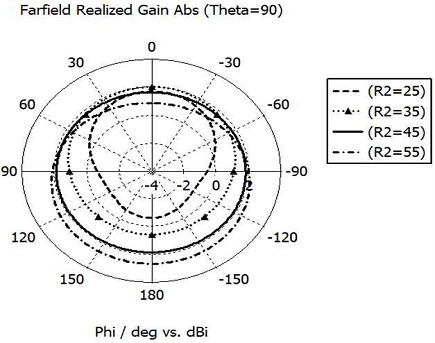
The final parameter to study is the parasitic strip's vertical portion length R2. The antenna's reflection coefficient is sensitive to R2 as shown in Fig. 25. Figs. 26 and 27 show the gain pattern versus R2 at ϕ = 0° and θ = 90° respectively. The pattern shape is sensitive to R2 and a good pattern symmetry is obtained when R2 is 45 mm.
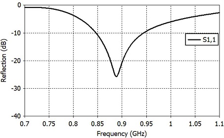
Based on the foregoing parametric analysis, we were able to find optimum dimensions of the proposed structure. The reflection coefficient of the proposed structure is less than -10 dB at 850-940 MHz as shown in Fig. 28.
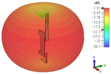
Fig. 29 shows the 3D absolute gain pattern of the proposed structure at 915 MHz. The pattern symmetry is good and the maximum gain is 1.91 dBi, which is not much different from 1.65 dBi of the dipole antenna alone shown in Fig. 6.
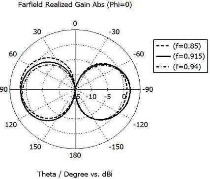
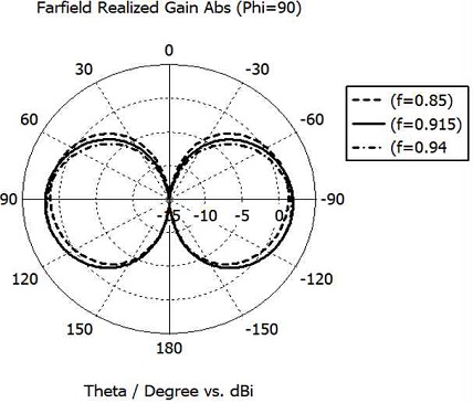
Figs. 30 and 31 show the gain patterns at 850, 915, and 940 MHz in the ϕ = 0° and ϕ = 90° planes respectively. The pattern symmetry is good at three frequencies while the best performance is obtained at 915 MHz. Using a pattern measurement tool in CST Studio Suite for the pattern in Fig. 30, we find that at ϕ = 0° and f = 915 MHz, the maximum gain of 1.71 dBi occurs at θ = 100° with 3-dB beamwidth of 97.5°, while at ϕ = 180°, the maximum gain of 1.82 dBi occurs at θ = -92° with 3-dB beamwidth of 81.7°.
At ϕ = 90° and f = 915 MHz, the maximum gain of 1.91 dBi occurs at θ = 95.0° with 3-dB beamwidth of 82.7°, while at ϕ = 180°, the maximum gain of 1.84 dBi occurs at θ = -96.0° with 3-dB beamwidth of 82.0°.
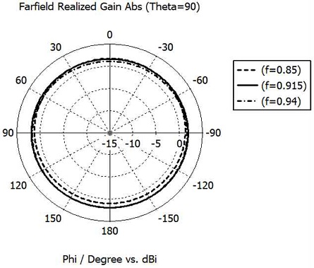
Fig. 32 shows the gain pattern in the θ = 90° plane at three frequencies 850, 915, and 940 MHz. The omnidirectional performance is best at 915 MHz. At 915 MHz, the maximum gain of 1.88 dBi occurs at ϕ = 108°, while the minimum gain of 1.62 dBi occurs at ϕ = -9.9°.
III. Conclusion
In this paper, we showed that the radiation pattern of a printed sleeve dipole placed parallel and close to a PCB is significantly distorted. To improve the dipole's gain pattern, we proposed a method that employs a metal wire and a bent metal strip placed at the bottom of the PCB. To illustrate the proposed method, we have used a small portable device operating at 900-MHz band with a PCB size comparable to the dipole antenna length. Optimum dimensions of the metal wire and the bent metal strip have been found from a parametric analysis using a commercial electromagnetic simulation tool. It has been shown that the distorted radiation pattern of the dipole antenna can be restored to the dipole's original pattern. Though the pattern distortion problem of a dipole near metallic objects needs to be solved on a case-by-case basis, authors believe that the method and idea presented in this paper offer useful insight for many similar situations.
Acknowledgments
This research was supported by Chungbuk National University Korean National University Development Project (2020).
References
-
Z. N. Chen, "Antennas for Portable Devices", New York: John Wiley & Sons, pp. 45-46, 2007.
[https://doi.org/10.1002/9780470319642]

-
Z. Zhang, "Antenna Design for Mobile Devices", 2nd Ed., John Wiley & Sons Singapore, pp. 163-167, 2017.
[https://doi.org/10.1002/9781119132332]

- K. Fujimoto and K. Ito, "Antennas for Small Mobile Terminals", Boston: Artech House, pp. 73-87, 2018.
- K. Fujimoto Ed., "Mobile Antenna Systems Handbook", Boston: Artech House, pp. 224-228, 2008.
-
J. B. Andersen and F. Hansen, "Antennas for VHF/UHF personal radio: a theoretical and experimental study of characteristics and performance", IEEE Trans. Vehicular Tech. Vol. 26, No. 4, pp. 349-358, Nov. 1977.
[https://doi.org/10.1109/T-VT.1977.23707]

-
T. Son and E.-s. Chang, "Monopole intenna for Korea PCS mobile phone handset", 10th Int. Symp. Ant. Tech. Appl. EM and URSI, Ottawa, Canada, pp. 20-23 Jul. 2004.
[https://doi.org/10.1109/ANTEM.2004.7860699]

-
Y. J. Cho, Y. S. Shin, S. H. Wang, and S.-O. Park, "A wideband internal antenna with dual monopole radiation elements", IEEE Antennas Wireless Propagat. Lett., Vol. 4, pp. 381-384, Nov. 2005.
[https://doi.org/10.1109/LAWP.2005.857969]

-
M. Tzortzakakis and R. J. Langley, "Quad-band internal mobile phone antenna", IEEE Trans. Antennas. Propagat., Vol. 55, No. 7, pp. 2097-2103, Jul. 2007.
[https://doi.org/10.1109/TAP.2007.898577]

- K. Ni and Y. Geng, "A compact six-element MIMO array for future 5G mobile terminal", '19 CSQRWC, Taiyuan, China, 18-21 Jul. 2019.
-
O. Delger, S. Li, and B.-C. Ahn, "Design of a quadruple-arm UHF dipole antenna fed by a collinear coaxial cable", Journal of KIIT, Vol. 18, No. 6, pp. 73-80, Jan. 2020.
[https://doi.org/10.14801/jkiit.2020.18.6.73]

-
S. S. Al-Bawari, M. F. Jamlos, P. J. Soh, S. A. A. S. Junid, M. A. Jamlos, and A. Narbudowicz, "Multiband slot-loaded dipole antenna for WLAN and LTE-A applications", IET Microw. Anennas Propagat., Vol. 12, No. 1, pp. 63-68, Jan. 2018.
[https://doi.org/10.1049/iet-map.2017.0008]

-
C. M. Peng, I. F. Chen, and C. H. Liu, "Multiband printed asymmetric dipole antenna for LTE/WLAN applications", Int. J. Antennas Propagat., Vol. 2013. Dec. 2013.
[https://doi.org/10.1155/2013/704847]

-
S. C. Jung, T. H. Jung, and J. M. Woo, "Design of sleeve dipole antenna for suppressing leakage current on a coaxial cable", IEEE Antennas Wireless Propagat. Lett., Vol. 13, Mar. 2014.
[https://doi.org/10.1109/LAWP.2014.2309655]

-
Y. Ma, "System embedded antenna for portable TVWS cognitive radio transceiver", IEEE Antennas Wireless Propagat. Lett., Vol. 14, pp. 265-268, Oct. 2014.
[https://doi.org/10.1109/LAWP.2014.2362127]

- D. Sasaki, S. Hayashida, K. Imamura, H. Morishita, and M. Usami, "A planar folded dipole antenna for handset", IEEE Int. Workshop Antenna Tech., Small Antennas Novel Metamater., Singapore, pp. 133-136, Mar. 2005.
-
L. Ntseane and B. Isong, "Analysis of LoRa/LoRaWAN challenges: review", 2019 IMITEC, Vanderbijlpark, South Africa, Nov. 2019.
[https://doi.org/10.1109/IMITEC45504.2019.9015864]

- Dragino homepage, https://www.dragino.com/products/lora-lorawan-end-node/item/155-lsn50-v2.html, . [accessed: 25 Jan., 2022]
- Advantech, WISE-3610 Wireless IoT LoRa Network Gateway data sheet, https://advdownload.advantech.com/productfile/PIS/WISE-3610/file/WISE-3610_DS(122220)20201222102228.pdf, . [accessed: 25 Jan., 2022]

2017. 1 : M. S. Degree, Electrical Eng., Power Engineering School of Mongolian University of Science and Technology
2019. 3 ~ present : Ph. D. Student, Radio and Communications Eng., Chungbuk National University
Research interests : Antennas, RF, Microwave

1987. 2 : B. A. Degree, Management, Sungkyunkwan University
2020. 9 ~ present : M. S. Student, Radio and Communications Eng., Chungbuk National University
Research interests : Antennas, RF, Microwave

2008. 2 : Ph. D., Dept. of Electrical Engineering, KAIST
2008. 3 ~ 2010. 2 : Senior Researcher, Samsung Electronics
2010. 3 ~ 2011. 8 : Assistant Professor, Wonkwang Univ.
2011. 9 ~ present : Professor, Dept. of Information and Communication Eng., Chungbuk National University
Research interests : Embedded systems, Software

2005. 4 : Ph. D., Dept. of Engineering, Cambridge University
2005. 8 ~ present : Professor, Dept. of Autonomous Vehicle System Engineering, Chungnam National University
Research interests : Flow induced noise, Cavitation, Computer vision

1992. 12 : Ph. D., Electrical Eng., University of Mississippi.
1992 ~ 1994 : Researcher, Agency for Defense Development
1995 ~ present : Professor, Radio and Communications Eng., Chungbuk National University
Research interests : Antennas, Applied electromagnetics

