Design of a Full Waveguide-Band E-Plane T-Junction Power Divider
Abstract
Waveguide power dividers are employed in a wide range of applications such as high-power microwave devices, particle accelerators, power-combiners in amplifiers, waveguide multiplexers, monopulse antenna comparators, and array antenna feed networks. A design is presented in this article for a power divider in E-plane of a rectangular waveguide which operates over the whole frequency range of the standard waveguide. The divider employs two linearly stepped ridges in the output waveguide for ease of manufacturing and does not have any other impedance-matching structures. As a result, the proposed power divider has an advantage of easy fabrication and high-power handling capability. Design results are presented for dividers with the narrow-to-broad wall width ratio (b/a) of 0.4, 0.5, and 0.6 in the rectangular waveguide so that they can be used for any standard WR-series rectangular waveguide.
초록
도파관 전력분배기는 고출력 마이크로파 장치, 입자 가속기, 증폭기에서의 전력합성기, 도파관 멀피플렉서, 모노펄스 안테나 비교기, 배열 안테나 급전회로망과 같은 다양한 용도로 사용된다. 본 논문에서는 표준 도파관의 전체 주파수 범위에 걸쳐 동작하는 전계면 전력 분배기의 설계를 제시하였다. 분배기는 가공의 편이성을 위해 2개의 선형 계단 리지를 사용하고 다른 임피던스 정합구조는 사용하지 않는다. 그 결과 제안된 전력 분배기는 용이한 가공과 고출력 동작능력의 장점을 가진다. 어떤 WR-계열 표준 사각 도파관에 대해서도 사용할 수 있도록 사각 도파관의 협벽과 광벽 폭 비 (b/a)가 0.4, 0.5 및 0.6인 경우 설계 결과를 제시하였다.
Keywords:
power divider, rectangular waveguide, E-plane, T-junction, optimum designI. Introduction
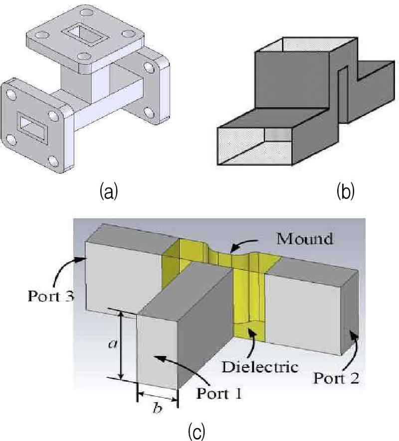
Power dividers operating at the whole recommended frequency range of a rectangular waveguide can be designed using various structures such as the Y-junction, posts, septa, and steps[1]-[4]. In space-limited and cost-constrained applications, it is preferable to employ dividers that occupy a small space with a simple shape. In some applications, a divider of branching type can be advantageous[3][4].
A divider without a septum or an input matching section shown in Fig. 1(a) shows input reflection coefficient of –15 dB to –10 dB[5]. A symmetric divider has been designed using a septum[6] in the junction or a matching section in the input waveguide.
The use of bifurcation in the junction shown in Fig. 1(b) provides a good impedance matching only over a narrow bandwidth[6]. Recently Bang and co-workers proposed a wideband divider shown in Fig. 1(c) empolying a round septum and a dielectric insert[7].
Wideband performance in a T-junction power divider can be obtained by using a wedge-shaped wave-branching structure in the junction shown in Fig. 2(a)[8]. Further bandwidth extension is possible with continuous or stepped impedance transformers shown in Fig. 2(b)[9] in the output waveguides. Isolation between output waveguides can be improved using a resistive card shown in Fig. 2(c)[10]. By offsetting the wedge, the ratio of the output can be controlled as shown in Fig. 2(d)[11].
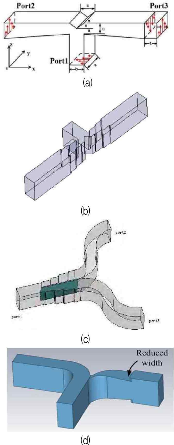
Wideband divider(a) Triangular matching structure (b) Stepped output guides (c) Resistive card (d) Variable division ratio
In this article, the authors present an E-plane divider design operating over the whole frequency range of the rectangular guide with reflection of less than –20 dB. The presented divider is much more compact and easier to fabricate than existing wideband designs. Also the proposed divider structure is simpler than existing works having only two steps in one of the side walls of the waveguide. Another differentiating feature of the proposed design is the use of a flat-topped branching part resulting in better manufacturability and higher mechanical strength.
The divider design has been carried out using widely-used electromagnetic simulation software CST Studio SuiteTM, the accuracy of which has been demonstrated in a large body of publications worldwide[12]-[14] that the simulation is enough to prove the validity of the design.
II. Power Divider Design
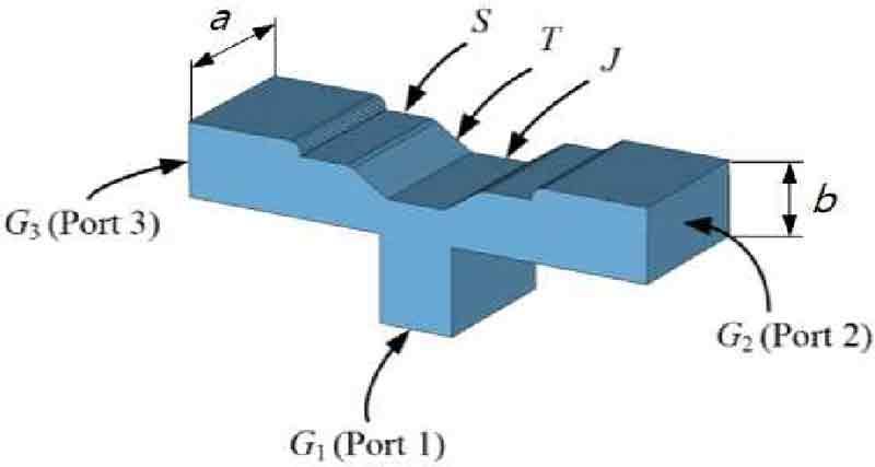
Fig. 3 shows the structure of the proposed power divider. The input waveguide G1 (Port 1) and two output waveguides G2 (Port 2) and G3 (Port 3) have the broad-wall dimension of a and the narrow-wall dimension of b. As in Fig. 4, at the junction the authors place a small waveguide section J with reduced height HJ and length LJ. The height of the junction waveguide J is linearly increased over a length of LT from HJ to HT by a tapered transition T. A stepped transition S connects the tapered transition T to the output waveguide (G2 and G3). The optimum dimensions of the power divider have been obtained from parametric analysis followed by computer-aided optimization. For fabrication, right-angle corners are rounded with radius of R.
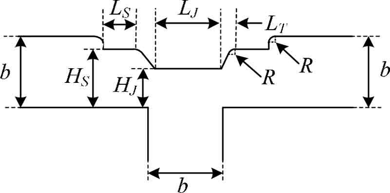
Design parameters of the divider(J : Junction waveguide, T : Tapered transition, S : Stepped transition)
Fig. 4 shows the divider's design parameters. Interior corners in the tapered transition T and in the stepped transition S are rounded with a radius of 0.16b for split-block fabrication using an end mill. Fig. 3 to 7 show results of the parametric analysis for the power divider in the WR-10 waveguide (75–110 GHz, a = 2.54 mm, b/a = 0.50).
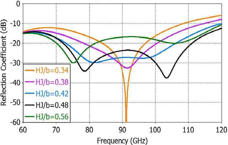
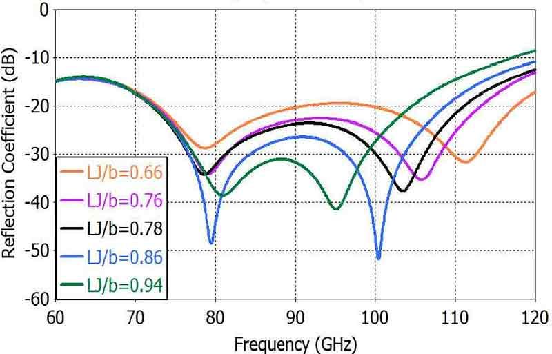
Fig. 5 and 6 show the reflection coefficient at the input waveguide (S11) versus the height HJ and length LJ of the junction waveguide J. The level of the input impedance matching and the bandwidth varies sensitively with HJ and LJ. Optimum HJ to b ratio is 0.48 resulting in reflection of less than -20 dB at 72 - 111 GHz. In Fig. 6, good reflection performance is obtained for LJ to b ratio from 0.66 to 0.86 with optimum being 0.78.
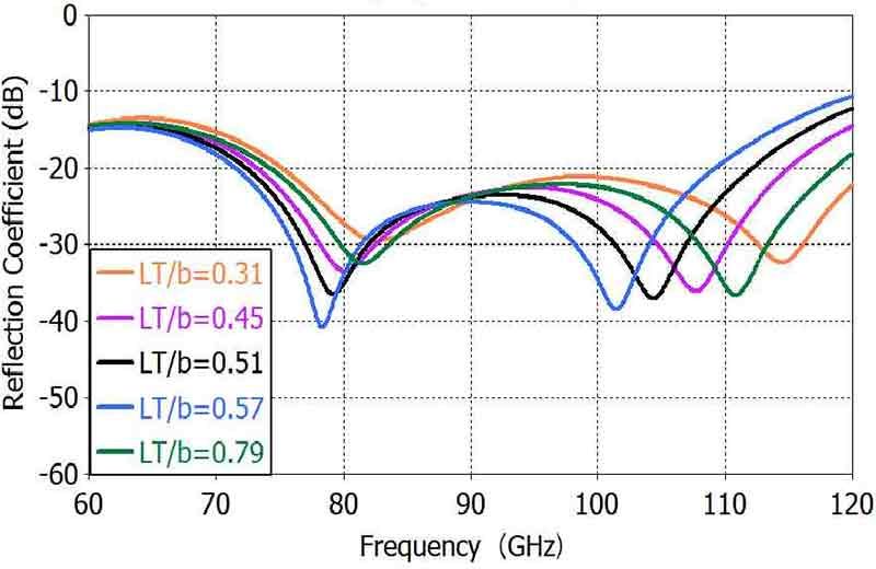
Fig. 7 shows the effect of the length LT of the tapered transition T. Reflection coefficient varies slowly with the variation of LT while the operating frequency range is shifted with variations in LT. Optimum value of LT to b ration is 0.51.
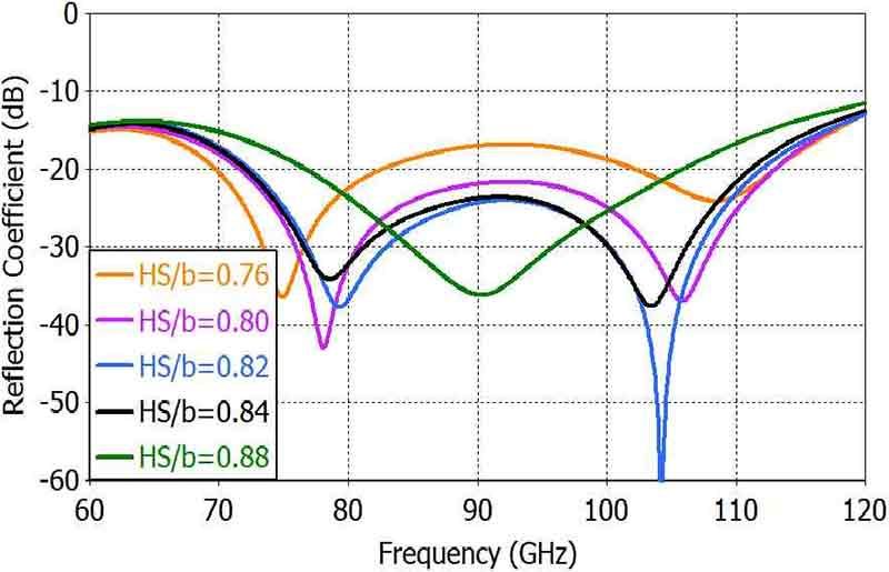
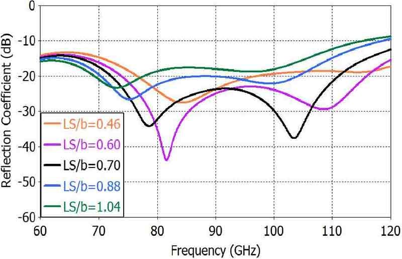
Fig. 8 and 9 show the reflection coefficient change versus the height HS and length LS of the stepped transition S. As in the case of the junction waveguide, the reflection performance varies sensitively with the changes in HS and LS. Good performance is obtained with HS to b ratio from 0.80 to 0.84. The optimum value of HS to b ratio is 0.84. The sensitivity of LS to reflection is less sensitive than in the case of HS. Optimum value of LS to b ratio is 0.70.
For fabrication with end-mill split-block method[15], concave corners in the divider's junction region are rounded with radius R of 0.16b. The value of 0.16b is a commonly accepted radius for split-block methods and is an optimal value that balances precision and ease of manufacture[15].
Near-optimum dimensions can be obtained from parametric studies. Divider's optimum dimensions have been obtained by using the automatic optimization functionality of CST Studio SuiteTM and are presented in Table 1 for the waveguide narrow-wall to broad-wall dimension ratio b/a = 0.4, 0.5, and 0.6. Optimum dimensions are different for different values of b/a. This is in contrast with the divider in the H-plane where the electric field and divider structure are uniform in the E-plane.
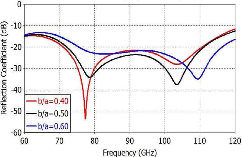
Finally, Fig. 10 shows the divider's reflection coefficient (|S11|) for b/a of 0.40, 0.50, and 0.60, which sufficiently covers the b-to-a ratio of standard rectangular waveguides. For b/a in the 0.40-0.60 range, the designed divider shows reflection coefficient of less than -20 dB at 75-110 GHz, which is the recommended operating frequency range of the WR-10 waveguide. The divider's transmission coefficient is given by (1-|S11|2)/2 from conservation of power since the divider has no internal loss.
III. Conclusion
A design has been presented for a divider in the E-plane of a rectangular waveguide which employs a T-junction and two linearly stepped ridges. The power divider is very compact while having reflection coefficient of less than –20 dB over the operating bandwidth of standard WR-series rectangular waveguides. Divider's dimensions have been obtained using CST Studio SuiteTM for the waveguide-wall aspect ratio b/a of 0.4, 0.5, and 0.6. Dimensions have been given in terms of the narrow-wall width b so that a divider can be designed for various standard rectangular waveguides. For reflection of significantly lower than -20 dB or for bandwidth greater than the recommended frequency range of rectangular waveguides, three or more linearly stepped ridges can be employed, whose dimensions can be obtained by optimization method presented in the paper.
Acknowledgments
This research was supported by Chungbuk National University Korea National University Development Project (2022)
References
- A. R. Kerr, "Elements of E-plane split-block waveguide circuits", AMLA Memo 381, 2001.
- J. Uher, J. Bornemann, and U. Rosenberg, "Waveguide Components for Antenna Feed Systems: Theory and CAD", Boston, MA: Artech House, Dec. 1993.
-
F. Arndt, I. Ahrens, U. Papziner, U. Wiechemann, and R. Wilkeit, "Optimized E-plane T-junction series power dividers", IEEE Transactions on Microwave Theory and Techniques, Vol. 35, No. 11, pp. 1052-1059, Nov. 1987.
[https://doi.org/10.1109/TMTT.1987.1133805]

-
I. Gómez, L. de Haro, B. Galocha, and J. L. Besada, "Optimized power dividers based on E-plane T-junctions", Microwave and Optical Technology Letters, Vol. 31, No. 2, pp. 118-123, Oct. 2001.
[https://doi.org/10.1002/mop.1375]

- Vector Telecom, "E-Plane Tee", http://www.vectortele.com/product_description.php?model_no=VT6WET, . [accessed: Nov. 18, 2024]
- J. Bornemann and M. Mokhtaari, "The bifurcated E-plane T-junction and its application to waveguide diplexer design", IEngineering, Physics, 2006.
-
Y. Bang, G.-Y. Ariunbold, and B.-C. Ahn, "A new E-plane T-junction waveguide power divider employing a dielectric insert", Journal of KIIT, Vol. 20, No. 1, pp. 121-128, Dec. 2021.
[https://doi.org/10.14801/jkiit.2022.20.1.121]

- X. Zhang, Y. Chen, Y. Xie, and L. Liu, "An improved E-plane waveguide power divider design for 94 GHz dual-pyramidal horn antenna", ACES Journal, Vol. 34, No. 12, pp. 1897-1903, Dec. 2019.
-
M. Zou, Z. Shao, J. Cai, L. Liu, and X. Zhu, "Ka-band rectangular waveguide power dividers", 2011 International Conference on Computational Problem-Solving (ICCP), Chengdu, China, pp. 375-377, Oct. 2011.
[https://doi.org/10.1109/ICCPS.2011.6092239]

-
H. Chen, X. Xie, and R. Xu, "An ultra wide band power divider/combiner based on Y-structure waveguide", 2010 International Conference on Microwave and Millimeter Wave Technology, Chengdu, China,, pp. 853-855, May 2010.
[https://doi.org/10.1109/ICMMT.2010.5525182]

-
F. Zhang, Q.-Y. Zhang, Y. Bang, and B.-C. Ahn, "Full waveguide-band E-plane power divider with high output power ratio", Journal of KIIT, Vol. 20, No. 2, pp. 117-122, Feb. 2022.
[https://doi.org/10.14801/jkiit.2022.20.2.117]

-
S. Xu, J. Heo, B.-K. Ahn, C.-S. Lee, and C.-C. Ahn, "Simulation-based approach to the matching of a dielectric-filled circular waveguide", Sensors, Vol. 24, No. 3, pp. 841, Jan. 2024.
[https://doi.org/10.3390/s24030841]

-
M. Simone, A. Fanti, M. B. Lodi, T. Pisanu, and G. Mazzarella, "An in-line coaxial-to-waveguide transition for Q-band single-feed-per-beam antenna system", Appl. Sci., Vol. 11, No. 6, pp. 2524, Mar. 2021.
[https://doi.org/10.3390/app11062524]

-
M. N. M. Kehn and P.-S. Kildal, "Miniaturized rectangular hard waveguides for use in multifrequency phased arrays", IEEE Transactions on Antennas and Propagation, Vol. 53, No. 1, pp. 100-109, Jan. 2005.
[https://doi.org/10.1109/TAP.2004.840519]

-
N. Jastram, M. A. Altarifi, L. Boskovic, and D. S. Filipovic, "On the split-block realization of millimeter-wave ridge waveguide components", IEEE Microwave and Wireless Components Letters, Vol. 28, No. 4, pp. 296-298, Apr. 2018.
[https://doi.org/10.1109/LMWC.2018.2808420]


1995. 8 : BS degree, Dept. of Business Administration, Chungbuk University
2016. 2 : MS degree, Dept. of Nano Semiconductor Eng., Chungbuk University
2019. 3 ~ present : Phd student, Dept. of Radio and Communication Eng., Chungbuk University
2015. 5 ~ present : CEO, NEO-SEMITECH Co., Ltd
Research interest : Electronic Circuit, Wired and wireless communication, Semiconductor

2021. 1 : MS degree, Dept. of Electronic Eng., Mongolian University of Science and Technology
2021. 3 ~ present : Phd student, Dept. of Radio and Communication Eng., Chungbuk University
Research interest : Antenna, Software

2010. 2 : BS degree, School of Information and Communication Eng., Chungbuk University
2012. 8 : MS degree, Dept. of Electrical Eng., Chungbuk University
2017. 8 ~ present : CEO, (C)TechBridge
Research interest : Circuit Design, Wired and wireless communication

2002. 2 : BS degree, Dept. of Computer Eng., Dongguk University
2016. 8 : MS degree, Dept. of Radio and Communication Eng., Chungbuk University
2023. 2 ~ present : Phd student, Dept. of Radio and Communication Eng. Chungbuk University
2004. 2 ~ present : Principal Researcher, KG Mobility Technology Research Center
Research interest : Antenna, Ratio application

2006. 2 : BS degree, School of Electrical and Computer Eng., Dongguk University
2008. 8 : MS degree, Dept. of Radio and Communication Eng., Chungbuk University
2011. 2 : Phd student, Dept. of Radio and Communication Eng. Chungbuk University
2018. 7 ~ present : Manager Hanbit EDS Co., Ltd
Research interest : IoT, RF Circuit, Antenna, Energy Harvest

2009. 2 : Phd degree, Dept. of Computer Eng., KAIST
2008. 3 ~ 2010. 2 : Senior researcher, Samsung Electronics
2011. 3 ~ present : Professor, School of Information and Communication Eng., Chungbuk University
Research interest : Embedded systems, computer architecture, mobile cloud

