Automated System for Cleaning Semiconductor Wafer
Abstract
The wafer cleaning process is essential to obtain high-quality semiconductors, and wafers are currently transported using a belt conveyor method. In this paper, a robot equipped with a vacuum suction gripper was used to minimize damage during wafer transfer. In addition, a cleaning system was implemented that separated the space between processes, and a vision inspection system was applied to detect wafer defects after the cleaning process. The performance of the system proposed in this paper was verified with the robot's repeatability of 0.011mm and 0.033mm on the left and right sides respectively, cycle time of 36.7s, damage rate during wafer processing of 0%, and wafer defect detection rate of 100%. The use of automated wafer cleaning and surface inspection equipment proposed in this paper is expected to minimize wafer damage and ultimately increase semiconductor yield.
초록
양질의 반도체를 얻기 위해서 웨이퍼 세정공정은 필수이며 현재 벨트 컨베이어 방식으로 웨이퍼 이송이 이루어지고 있다. 본 논문에서는 웨이퍼 이송 중 손상을 최소화하기 위하여 진공 흡착 그리퍼가 장착된 로봇을 사용했다. 또한, 공정 간의 공간을 분리하여 별도의 세정 시스템을 구현했으며 세정 공정 이후 웨이퍼 불량을 검출하기 위해 비전 검사 시스템을 적용했다. 본 논문에서 제안하는 시스템의 성능은 로봇의 반복성이 좌, 우 각각 0.011mm, 0.033mm, 사이클 타임이 36.7s, 웨이퍼 가공 중 손상률이 0%, 웨이퍼 불량 검출률이 100%로 검증됐다. 본 논문에서 제안하는 자동화된 웨이퍼 세정 및 표면 검사 장비의 활용은 웨이퍼 손상을 최소화하고 궁극적으로 반도체 수율을 높일 수 있을 것으로 기대된다.
Keywords:
wafer, semiconductor, CMP, transfer robot, vision systemⅠ. Introduction
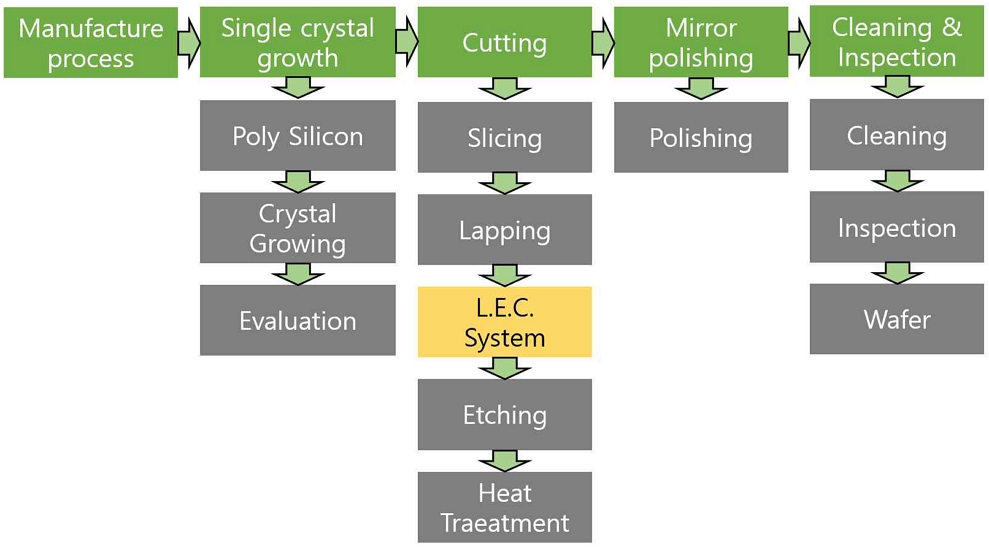
Semiconductors are used in many areas of daily life, such as mobile phones, laptops, and cars, so it is difficult to imagine life without semiconductors. Wafers exist as a key material for semiconductor integrated circuits[1]-[2]. Since the semiconductor process deals with very fine processes, even if a trace amount of impurities such as metals and organic substances exist on the wafer surface, the yield of semiconductor products may decrease and the product may malfunction, ultimately affecting the competitiveness of the semiconductor industry[3]. To obtain high-quality semiconductors, a wafer cleaning process is essential [4]. Fig. 1 shows the wafer processing process, with the wafer cleaning process shown in yellow. The wafer cleaning process is also called L.E.C(Liquid Encapsulated Czochralski) in the field[5]. The L.E.C. process generally proceeds in the following order: water cleaning, brush cleaning, and air dry cleaning. Currently, wafer transfer and cleaning operations are performed continuously in the field. A conveyor system is used when transferring wafers[6]. When transported through a conveyor, vibration occurs and shock is applied to the wafer, causing damage, etc., which frequently occurs. If a problem occurs with one wafer, the process itself may have to stop due to the stacking of subsequent work-in-process products. As a result, management costs for the process increase, processing costs increase due to defects, and yields decrease. Recently, in the semiconductor manufacturing process, the intelligentization and smartization of production facilities is continuously progressing due to the spread of smart factories and strengthening cost competition. Damage to wafer defects must be minimized in the wafer cleaning process, which is essential in the semiconductor manufacturing process, and an automated system is required for this process[7]. This paper discusses wafer cleaning and surface inspection automation equipment. The existing wafer cleaning process is carried out using a conveyor method when transferring the wafer, and damage to the wafer occurs due to shock during transfer. Additionally, in the existing method, the wafer cleaning, wafer brushing, and wafer drying processes were open, causing problems with interference and cross-contamination between processes[8].
Accordingly, this paper minimizes wafer damage by safely and quickly transporting wafers between each process using a vacuum adsorption robot system, and proposes a cleaning system with a separate compartment structure to prevent interference and cross-contamination between processes[9]-[12]. After cleaning the wafer, a vision inspection was developed to inspect the wafer surface for contamination and damage[13]. As a result, it is expected that using the automatic inspection equipment proposed in this paper when cleaning wafers will minimize wafer damage and ultimately increase semiconductor yield.
Ⅱ. System configuration
The equipment proposed in this paper consists of a wafer cleaning tank, wafer transfer robot, three-stage separate wafer cleaning system, D.I.W(De-ionized Water) supply system, vision inspection system, and CST(Controlled Start Transmission) unloading.
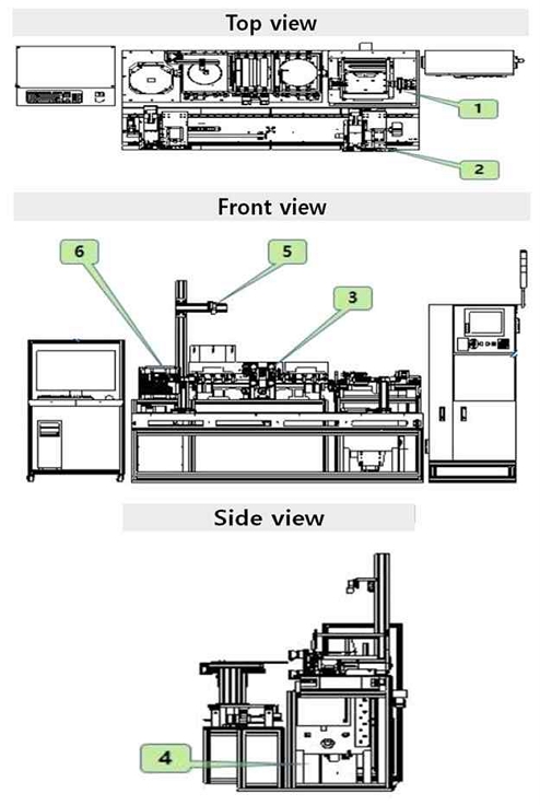
The top, front, and side views of the system are shown in Fig. 2. The picture is divided into six parts. Number 1 in the picture is the wafer cleaning bath, which consists of ultrasonic waves and a heating device for wafer cleaning. 2 is a wafer loading robot, which is a robot that transfers wafers. 3 is the part where the wafer is cleaned using the wafer cleaning system. 4 is the D.I.W supply part and functions as an autodrain system. 5 is a vision system that inspects the appearance of the wafer and detects defects and damage. 6 is the cst transfer, which is the part that discharges the finished product.
Fig. 3 shows the process of wafer cleaning. In the wafer cleaning process, when a wafer is input, ultrasonic cleaning is performed, followed by washing and drying, and finally discharge.
Ultrasonic cleaning is performed in the wafer cleaning bath and the temperature of the cleaning water is automatically adjusted. The cleaning and drying process consists of a three-stage separate wafer cleaning system to prevent interference and cross-contamination between processes. The wafer transfer process utilizes a robot equipped with a vacuum suction tool.
2.1 Wafer transfer method
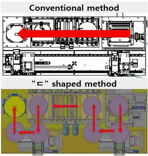
The wafer transfer method is shown in Fig. 4. The existing wafer transfer method is done in a straight line, but in this study, transfer is done in a “ㄷ” shape. In the existing method, it is difficult to maintain and check the operating status because the wafer transfer drive unit is internal, but by changing it to a “ㄷ” shape, the drive unit is exposed to the outside, making it advantageous to check maintenance and operating status.
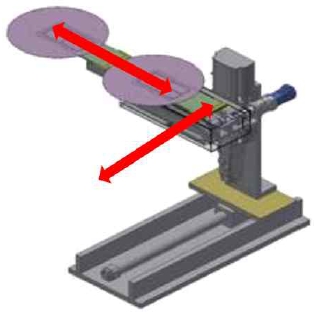
The robot used for wafer transfer is an cartesian robot, as shown in Fig. 5. Many wafer defects occurred due to wafer transfer and cleaning work performed using the existing belt conveyor method, but in this paper, wafer damage was minimized by using a vacuum suction tool.
2.2 Wafer cleaning system
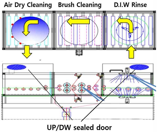
The wafer cleaning process consists of D.I.W rinse, brush clean, and air dry clean processes. Fig. 6 shows the transport path of the wafer cleaning process. The existing wafer cleaning process is an open, integrated process that causes interference and cross-contamination between processes, but in this paper, the wafer cleaning process is structured in three independent spaces to prevent interference and cross-contamination between processes. The D.I.W rinse part has a nozzle that sprays water from the upper and lower parts. Brush cleaning uses a base brush that minimizes damage to the wafer and applies a two-fluid nozzle. The air dry cleaning part removes remaining foreign substances and moisture from the wafer surface using warm air.
2.3 Vision system
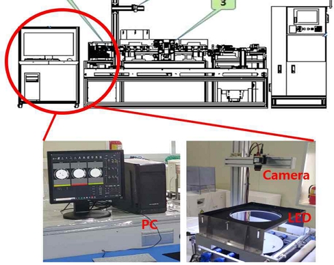
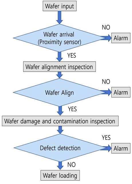
The existing process did not have a vision inspection system after the wafer cleaning process was completed. In this paper, a vision inspection system was added to determine and classify the presence or absence of defects on the wafer surface after the cleaning process is completed[14]. The configuration diagram of the vision system is shown in Fig. 7. A 5-megapixel area camera is installed at the top to acquire wafer images, and LED(Light-emitting diode) is installed to obtain uniform image quality even in a complex environment. The acquired images are transferred to the PC(Personal Computer), and the vision inspection program on the PC classifies whether the wafer is defective or normal. Fig. 8 shows the work flow of the vision inspection program.
After confirming that the wafer is located under the camera through a proximity sensor, the wafer is inspected for alignment, the wafer is inspected for contamination and damage, and if there are no problems, the wafer is loaded.
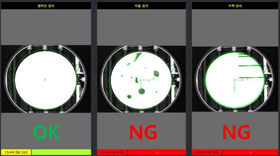
Fig. 9 shows the vision inspection program. If it is a normal product, it is marked in green, and if it is defective, it is marked in red.
Ⅲ. Performance verification
Considering the size and weight of the development equipment, formal testing was conducted after evaluation by the Daegu Mechanical Parts Research Institute in Korea. The results of performance verification are shown in Table 1. The robot repeatability evaluation method was evaluated by measuring the repeatability of the transfer robot of the wafer cleaning and surface inspection equipment using a laser tracker device. The repeatability performance of the existing transfer robot was 0.15mm, and the repeatability performance of the method proposed in this paper was 0.033mm for the right robot and 0.011mm for the left robot, which improved the repeatability performance by 0.117mm and 0.139mm, respectively. Cycle time is the process time required to move 10 wafers using a robot using wafer cleaning and surface inspection equipment, then wash the surface, complete air dry clean, and load the cassette. The cycle time for manual work was about 120 seconds, and the automated equipment proposed in this paper took an average of 36.7 seconds. Using the method proposed in this paper, cycle time can be reduced to 30.58% of the cycle time required during manual work. Therefore, it can be processed about 3.2 times faster than the time taken manually. The damage rate during wafer processing was evaluated by repeating the vacuum suction and movement of the transfer robot 100 times to measure falling rocks, poor adsorption, and poor seating.
As a result of the test, it was confirmed that the damage rate was 0% and no wafer damage occurred. System operation stability rate was evaluated by repeating the process of transferring 10 wafers, surface cleaning, air drying, and cassette loading 10 times to evaluate the number of errors. As a result of the performance measurement, the system operation stability was 100%, confirming that the automation system was stable. Surface contamination detection rate was evaluated for surface defects of the wafer using a vision inspection device. Damage detection rate was evaluated to determine whether wafer damage was properly detected using vision inspection equipment. Damage detection rate and wafer surface contamination detection rate were 95% during visual inspection, and 100% for the method proposed in this paper. It was confirmed that the method proposed in this paper showed about 5% better performance than visual inspection.
Ⅳ. Conclusion
The wafer cleaning process consists of D.I.W Rinse, Brush Clean, and Air Dry Clean processes. While the existing process was an open process, the system proposed in this paper used a three-stage process separation with a compartment structure, which prevented interference and cross-contamination between processes. In addition, wafer damage was minimized by transferring wafers using a vacuum suction robot instead of using a conventional conveyor belt. Immediately after the wafer cleaning process, vision inspection is used to inspect the wafer for defects or damage. When the performance of the system proposed in this paper was verified, including robot precision, cycle time, and defect detection rate, it was confirmed that the results were higher than the existing performance. The repeatability of the robot has become 0.117 mm more accurate for the right robot and 0.139 mm more accurate for the left robot than the existing performance. The cycle time took an average of 36.7 seconds, which is about 3.2 times faster than the time required manually. The damage rate during wafer cleaning was 0%, which confirmed that no wafer damage occurred, and as a result of the system stability performance test, it was confirmed to be stable at 100%. Using vision inspection, the damage detection rate and wafer surface contamination detection rate were 100%, confirming that all defects were detected. The method proposed in this paper promotes the development of wafer cleaning process technology, establishing a foundation for high-speed, low-damage mass cleaning and smart manufacturing. Furthermore, cost savings can be expected by minimizing manpower input and improving process operation rates, and it is believed that if a lot of data is secured in the future, it will be possible to use it to build a smart factory.
Acknowledgments
This research was supported by Kumoh National Institute of Technology(2022~2024)
References
-
A. Bidiville, K. Wasmer, J. Michler, P. M. Nasch, M. V. Meer, and C. Ballif, "Mechanisms of wafer sawing and impact on wafer properties", Progress in photovoltaics, Vol. 18, No. 8, pp. 563-572, Nov. 2010.
[https://doi.org/10.1002/pip.972]

-
S. G. Ghoi, S. J. Lee, and C. S. Nam, "Enhanced Machine Learning Preprocessing Techniques for Optimization of Semiconductor Process Data in Smart Factories", The Journal of The Institute of Internet, Broadcasting and Communication (IIBC), Vol. 24, No. 4, pp. 57-64, Aug. 2024.
[https://doi.org/10.7236/JIIBC.2024.24.4.57]

- J. W. Lee, B. J. Lee, and J. J. Lee, "Wafer Position Recognition System of Cleaning Equipment", Journal of Korea Multimedia Society, Vol. 13, No. 3, pp. 400-409, Mar. 2010.
- B. Bera, "Silicon Wafer Cleaning: A Fundamental and Critical Step in Semiconductor Fabrication Process", International Journal of Applied Nanotechnology, Vol. 5, No. 1, pp. 8-13, 2019.
- W. W. Jung, Y. S. Lee, and C. H. Chun, "An Experimental Study on the Oscillatory Convection in a Model Liquid Encapsulated Czochralski(LEC) Crystal growth system", JTransactions of the KSME, Vol. 2, No. 2, pp. 906-911, Jan. 1998.
- D. W. Kim, "Design of the Magnetic Levitation Transportation System on Semiconductor Manufacturing Line", Hongik University Master's Thesis, pp. 9-10, 2003.
- S. W. Choi and J. S. Lee, "Real-Time Scheduling System Re-Construction for Automated Manufacturing in a Korean 300mm Wafer Fab", Journal of Intelligence and Information Systems, Vol. 15, No. 4, pp. 213-224, Dec. 2009.
- Y. J. Ji, J. I. Park, Y. H. Lee, and Y. H. Kim, "Development of a Multi-Separate Processing Robot-Based Wafer Cleaning Bath", Proc. of KIIT Conference, Jeju, Korea, pp. 144-145, Jun. 2022.
- J. S. Choi, "A study on the measurement and comparison of vacuum suction performance according to the shape of suction cups for robot automation in the logistics industry" Mokwon University Master's Thesis, pp. 6-32, 2023.
- S. Y. Kwon, Y. H. Kim, J. I. Park, and Y. H. Lee, "Development of Wafer Cleaning Automation Equipment using Vacuum Adsorption Robot System", Proc. of KIIT Conference, Jeju, Korea, pp. 203-204, Dec. 2022.
-
M. Zhang, W. Tao, W. Fisher, and T. J. Tarn, "An industrial solution to automatic robot calibration and workpiece pose estimation for semiconductor and gene-chip microarray fabrication", The Industrial robot, Vol. 33 No. 2, pp. 88-96, Mar. 2006.
[https://doi.org/10.1108/01439910610651383]

-
T. Katsuma, "Vacuum manipulator for semiconductor manufacturing equipment", The Industrial robot, Vol. 29, No. 4, pp. 324-328, Aug. 2002.
[https://doi.org/10.1108/01439910210441119]

-
Y. D. Park, J. S. Kim, and H. N. Joo, "The GPU-based Parallel Processing Algorithm for Fast Inspection of Semiconductor Wafers", Journal of Institute of Control, Robotics and Systems, Vol. 19, No. 12, pp. 1072-1080, Dec. 2013.
[https://doi.org/10.5302/J.ICROS.2013.13.9037]

-
D. J. Jeong and H. Huh, "Deep Learning-based X-ray Inspection for Battery Defect Detection", The Journal of The Institute of Internet, Broadcasting and Communication (IIBC), Vol. 24, No. 2, pp. 147-153, Apr. 2024.
[https://doi.org/10.7236/JIIBC.2024.24.2.147]


2019. 02. : M.S degrees in Department of Electrical Engineering, Kumoh National Institute of Technology
2022. 09. ~ Present : Ph.D candidate in Department of Electrical Engineering, Kumoh National Institute of Technology
Research interests : Digital SoC, Image Processing, Verilog HDL

2010. 02. : PhD degree in Department of Industrial Management, Kumoh National Institute of Technology, Korea
2014. 09. ~ Present : Professor of Department of IT Convergence, Kumoh National Institute of Technology
Research interests : Industrial System, 3D Printer

2022. 07. : M.S degrees in Department of Electronic & Electrical Engineering, Kumoh National Institute of Technology
2009. 12. ~ Present : CEO of Sejung Robot Co., LTD
Research interests : Robot, Control System, Automation System

2023. 09. ~ Present : Graduate Student in the Department of Smart Convergence Engineering, Kumoh National Institute of Technology, Korea
2023. 03. ~ Present : CEO of NAVOROS Co.
Research interests : Drone Safety Control Systems, Drone Airbags, Smart Goggles

2012. 03. : Ph.D Degree, University of Leeds Business School
2023. 03. ~ Present : Professor of Department of IT Convergence, Kumoh National Institute of Technology
Research Interest: Digital Transformation, Value Chain Analysis, Tech Convergence

