FPGA Design for Implementation of Analog Output Board with Eight Voltage Output Channels
*Department of Electronic Engineering, Graduate School, Kumoh National Institute of Technology**Department of IT Convergence, Kumoh National Institute of Technology
***School of Electronic Engineering, Kumoh National Institute of Technology
Abstract
In this paper, we design FPGA to control a DAC board that can output analog voltage upto 8 channels. The board receives 16-bit data from the host and transmits it to 8 Digital-to-Analog-Converters (DACs) for analog outputs. The FPGA functions as an intermediate between the host and the DAC, and each DAC can be independently configured and the data flow can be controlled accordingly. To this end, the FPGA has 8 first-in first-out (FIFO) buffers that can store 128 samples, and requests data through the interrupt to the host to seamlessly supply data for each DAC channel. In the existing DAC boards, if the input signal is momentarily cut off or noise is generated, the signal may be distorted. In this paper, accurate timing is provided because data flow is controlled by FPGA using Hardware Description Language (HDL). In addition, this method has the advantage of being able to be modified easily along with price competitiveness.
초록
본 논문에서는 최대 8개 채널로 아날로그 출력을 내보낼 수 있는 DAC 보드의 제어를 위한 FPGA를 설계한다. 보드에서는 16비트의 데이터를 호스트로부터 입력 받아 8개의 DAC(Digital-to-Analog-Converter)에 전달함으로써 아날로그 출력을 내보낸다. FPGA는 호스트와 DAC 사이의 중간에 위치하며, 각 DAC를 독립적으로 설정하고 이에 맞추어 데이터의 흐름을 제어할 수 있다. 이를 위해 FPGA에는 128개의 샘플을 저장할 수 있는 8개의 FIFO(First-in First-out) 버퍼가 있으며 호스트와는 인터럽트 방식을 통해 데이터를 요청하여 각 DAC 채널을 위한 데이터를 끊김 없이 공급한다. 기존의 DAC 보드들은 입력된 신호가 순간적으로 끊기거나 노이즈가 발생한다면 신호의 왜곡이 발생하기도 한다. 본 논문에서는 HDL(Hardware Description Language)을 사용한 FPGA로 데이터의 흐름을 제어하기 때문에 정확한 타이밍을 제공한다. 또한 이러한 방식은 가격 경쟁력과 함께 수정이 가능하다는 장점이 있다.
Keywords:
FPGA, signal conversion, multi-channel, data calibration, compensating for signal distortion, DACⅠ. Introduction
Most of electronic products these days use many Analog-to-Digital Convertors and/or Digital-to-Analog Convertors. In particular, the DAC is used to drive voltage-controlled devices by converting digital data into analog signals. A device that accepts an analog signal as an input is, for typical example, a speaker or a motor.
In the case of an existing DAC board used in a specific product, noise or signal distortion may exist when digital data transit abruptly. Fig. 1 shows the distortion of the digital signal when the signal data is changed, and Fig. 2 shows the distortion of the digital signal due to noise. The most important point of the DAC board is to reduce data loss and noise as much as possible and preserve the original data when converting digital signals to analog signals. In the case of a DAC board, it is impossible to replace the function unit used in the existing product if it cannot output signals properly or compensate for its shortcomings.
If DAC operates as single channel, the output efficiency decreases[1]. In the case of multi-channel, if only the same operation is performed in multiplexing, the existing workload may increase by the number of channels, but if each channel cannot be controlled, the efficiency is also reduced. Therefore, it should be designed to allow a dedicated configuration for each channel, and the speed of the DAC operation each channel should be adjustable respectively[2][3]. For speed adjustment, the conversion time should be set to allow the user to adjust the speed according to the desired channel when performing the DAC[4]. In the step of converting digital data to analog data, a correction step is required to control the speed as well as to prevent data loss or incorrect transmission. In the correction step, an operation is performed to correct the existing digital data by using the offset data, and it is transmitted to the DAC[5]. The corrected data is output according to the speed set above, and the data is continuously transmitted to the DAC using Serial Peripheral Interface(SPI) communication[6][7].
In this paper, we propose a module that data-corrects the signal entering the input of the DAC board using 8 multi-channels, controls the DAC interval, and delivers the data to the DAC. For compatibility with the existing DAC board, the ROM was configured to have ID data, and it was set to match the DAC board used in the existing product[8]. The distortion signal generated in the existing digital data signal was output as a linear waveform using the proposed method. It was verified using FPGA, and it was confirmed whether the input signal was normally output through simulation and emulation.
This paper is structured as follows. Section 2 describes the data input method and FIFO, and Section 3 describes the register map used in this system. Section 4 describes the structure and algorithm of the overall system. Section 5 presents the experimental results, and finally, conclusions and outlines for future research directions are drawn in section 6.
Ⅱ. Related Works
Big endian method is used for this module[9]. The big endian is the convention used in the Motorola 68000 family of microprocessors and refers to the VMEbus rule[10]. In big endian, low-order bytes are stored at odd byte addresses, and byte access is performed at odd address locations. Little endian has a structure in which the lower byte is stored using an even byte address. Existing products have a carrier board and a method of mounting modules. In the case of this paper, the system is configured using the FPGA in the module and the corresponding module is mounted on the carrier board. The use of the module on the carrier board requires access to 8-bit data using an even address location. For VMEbus carriers, odd address locations must be used. Multiple modules can be mounted on the carrier board, which are identified by ID. For each module, there is an identification ID according to the specification. The ID memory area includes up to 32 bytes of information, and fixed and variable information may exist in it. In the case of fixed information, identifiers, model numbers, and manufacturer's identification codes are included, and variable information has a structure in which unique information required by the module is included.
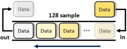
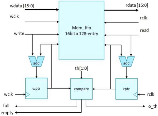
The buffer used in this module is a FIFO(First-In, First-Out memory), and input data is stored in the order in which it is input. When data is output, the first stored data is processed in order by reading the memory. Asynchronous FIFO is used, in case the clock used to read or write data is different. As shown in Fig. 3, FIFO uses 16-bit data, 7 address values, and 128 samples.
Ⅲ. Register Map
Register map is made similarly to be compatible with the existing DAC board. Unnecessary functions are dealt with in different ways depending on the situation. In the case of a register map, the size consists of 16-bit data and an 8-bit address, the entire address is not used, and a partial address is used[11][12]. The data in the register map can be written or read by the CPU using the system bus[13][14]. The configuration of the register map can be divided into three main categories: control, status, and data.
3.1 Status and Control Part of Register Map
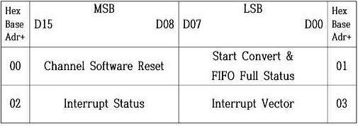
Fig. 4 shows the basic state and control part of the register map. The Channel Software Reset in Fig. 4 is used to reset each of the eight multiple channels. As shown in Fig. 5, if the 15th to 8th data bits are set to 1, a software reset is performed for each channel. When software resets, the counter values of individual channels, control registers, and FIFO buffers are cleared. Using software reset is also useful for initializing in case of an existing malfunction.
In the case of Start Convert & FIFO Full status in Fig. 6, there are two functions. When 7~0 of data bits are set to 1, conversion of individual channels is started. After each data is corrected and stored in a register, the data is transmitted through SPI communication. However, in order to transmit a channel, the FIFO register of each channel must be set.
In fact, channel conversion starts at least 6.625us after the Start Convert bit is set, but it is stable to set it to proceed after 10us. The register is also used to indicate the FIFO status of the currently used channel. In this case, the set bit of each channel indicates that the data is full, and data transmission is not approved. Data transfer here refers to writing additional data in the CPU. It is important to avoid writing additional data to the FIFO buffer because data transfer may not be acknowledged and a system bus error may occur. In the case of the register in Fig. 4, it is designed so that data can be written in 16 bits or 8 bits. The entire state is cleared upon software or hardware reset.
3.2 Interrupt Part of Register Map
In the Interrupt Status of Fig. 7, data bits 15~8 indicate the interrupt status. The interrupt condition of each channel occurs when the data of the FIFO is smaller than the set reference value. In case of interrupt, it can be turned on or off through the interrupt enable signal.
In the case of the Interrupt Vector in Fig. 8, it can be used as a pointer in the routine handling interrupt. The size of the vector is 8 bits, as allocated by the register map, and can be used to point to one of 256 locations.
3.3 Calibration factor part of register map
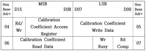
The data related to the calibration coefficient of the register map in Fig. 9 is used to fetch the data stored in EEPROM and correct the FIFO data.
The calibration steps can adjust and improve the accuracy of the uncalibrated data sent by the software. There is a unique offset and gain correction factor for each channel, which helps with data correction. The existing method determines whether to read or write data to the data of address 04 and puts the address value. Depending on the value to be read or written, the data in address 05 is written or the data stored in number 06 is displayed. Since this method has to go through the EEPROM, there is a disadvantage in that it is slow in transmitting and receiving data. To compensate for this, the RAM was configured to read or write data directly. The data correction method is as in Eq. 1.
| (1) |
The input data used to derive the "result" in Eq. 1 is as follows. In Eq. 1, Data refers to the value input from the CPU, which is software. In the case of gain, it refers to the value obtained by dividing the error value of the gain stored in the memory by the value of 262,144. Offset refers to the value obtained by dividing the offset error value stored in the memory by 4. Volts vary depending on the range of voltage used. If the voltage used is polarity, -5V to +5V, it has a value of 0, but if it is unipolar, 0 to 10V, it has a value of 32,768.
3.4 FIFO Control Part of Register Map
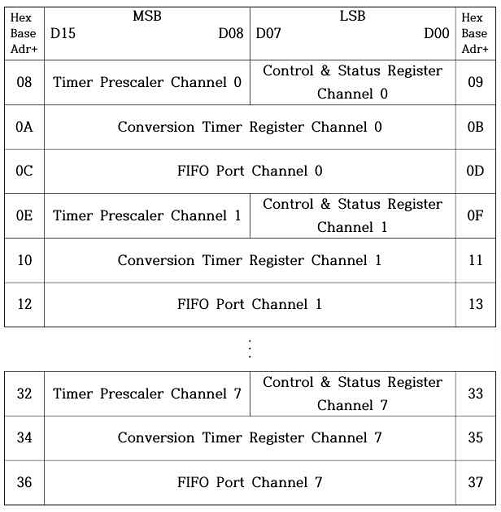
The channel register of the FIFO is shown in Fig. 10. It is composed of 8 channels, and each channel has 4 sections of FIFO, and is equally composed of registers related to control / status, DAC interval, and FIFO buffer. Through this, each channel can operate in a setting independent of other channels. Each section consists of an 8-bit control status register, an 8-bit timer prescaler, a 16-bit conversion timer and a 16-bit FIFO buffer.
The status and control registers are used to indicate the status of the FIFO as shown in Fig. 11. Bit 0 indicates the empty state of the FIFO. Bits 2~1 determine whether to use FIFO, single mode, continuous mode, or whether to use external trigger input when outputting FIFO. Bit 3 is used to select whether to use as input or output when using an external trigger. Bit 4 determines whether the corresponding channel uses interrupt. Bits 6~5 determine whether to generate an interrupt when the number of data in the current FIFO is less than how many data are present in the FIFO Since there are 2 bits, 4 can be selected, and either not used, or 4, 16 or 64 can be selected. Bit 7 is not used.
In the case of the timer prescaler in Fig. 12, it is used together with the conversion timer. Here, in the case of the timer prescaler, the hexadecimal value of 35 is the minimum value. If a value smaller than this is applied, there is a risk of malfunction. When this is applied, conversion starts at 6.625us intervals, which can achieve a speed of about 150KHz. When converting to 150KHz, the conversion accuracy is lowered, so the recommended conversion speed for the existing module is 100KHz.
That is, 10us is recommended. Eq. 2 is used to calculate this value, where the unit of the calculated value is microsecond.
| (2) |
Based on the input 8MHz clock, the value of the timer prescaler and the conversion timer value are multiplied, and the conversion time is obtained by dividing by 8. Here, the range of the timer prescaler value has a decimal value of 53~255 as mentioned in the register map, and the range of the conversion timer value has as much as 1~65,536 data. Using Eq. 2 when the timer prescaler value is 53 and the conversion timer value is 1, a value of 6.625us is derived, but the minimum value is redefined as 10us because the conversion accuracy is poor. To this end, the initial value is set when the value of the timer prescaler is 80 and the timer value is 1.
Each channel has a dedicated FIFO buffer that can hold 128 samples of data. FIFO data is used for data transmission, and the size is 16 bits. When starting to write new data, care must be taken not to full the FIFO. If there are 128 samples of data in the FIFO, additional data should not be written. Writing additional data may cause an error. To avoid this error, you can read the FIFO Full flag bit before writing the FIFO. A software or hardware reset can also be implemented to clear the FIFO.
As mentioned earlier, it is good practice to enable interrupts through the threshold of interrupts when the FIFO is almost empty. When interrupt occurs, the number of new data should be written to the FIFO by subtracting the existing threshold from the total number of data. Any remaining addresses are not used.
Ⅳ. System Structure
4.1 Overall System Structure
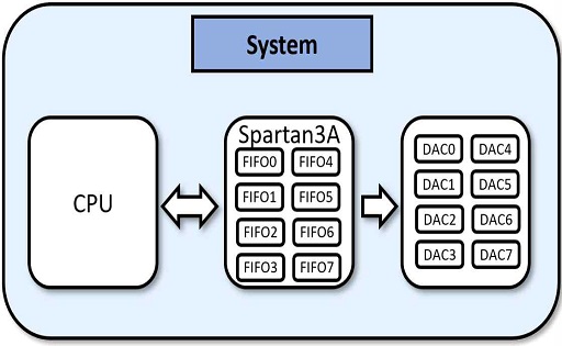
The structure of the whole system is shown in Fig. 13. CPU, Spartan 3A, and DAC chip exist in the whole system. The CPU is used to change the initial values of various register maps and FIFO settings, or to perform status and control. The internal structure of FIFO is configured as shown in Fig. 14. It also serves to supply data when an interrupt occurs. In Spartan 3A[15][16], there is a bus system and register map to communicate with the CPU mentioned above, and an SPI module for communicating with FIFO and DAC of 8 channels. In order to operate 8 channels independently, it is used to transmit data to the DAC using the associated register map and 1 SPI communication that can set the mode and data transmission period of 1 FIFO per each channel.
4.2 Algorithms
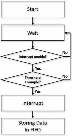
The flowchart of the algorithm is shown in Fig. 15. When the system power is applied and clock and reset are applied, the system operates. According to the flowchart, it is judged whether there is data in the FIFO, and if it is not Full, the data is stored in the FIFO in order. If all 128 samples of data are saved, no additional data is saved. When the Start Convert signal of each channel is generated, the data is sequentially retrieved from the FIFO and the data is corrected. The corrected digital data is stored in the FIFO Port of the FIFO register of each channel. When outputting data, it loads and outputs data from the aforementioned FIFO Port.
Two main modes are used to output data, single mode and continuous mode. The single mode is a structure that outputs the last pointer value of the FIFO whenever the Start Convert signal occurs. In the continuous mode, when the Start Convert signal is generated, the FIFO pointer value is incremented by 1 at regular intervals to sequentially export data. In the case of single mode, since only single data is used, a specific voltage value is displayed by outputting only the data value when outputting. In the continuous mode, since continuous data is output, a sine wave or other waveform is output.
In the case of SPI, data is exchanged between one master and several slaves, but in this system, there is no reason to return the digital data output to the DAC, so the MISO (Slave Output Master Input) pin is removed. Other signals such as SCLK, MOSI (Master Output Slave Input), SS (Slave Select) or CS (Chip Select) are used. Due to the characteristics of the DAC chip, when outputting data, the data is transferred using SPI communication, and the data is transferred while making the LDAC (Load DAC) signal of each channel LOW. SPI period setting is determined by calculating the values of Timer Prescaler and Conversion Timer of the FIFO register of each channel. In this case, it is a multiplication structure, but an operation is performed using a double counter.
When performing SPI output, additional correction is required for the corrected data. If the output range of ADC is positive, it helps to output positive data by adding the value of 16384.
4.3 Interrupt Signal Generation Routine
As illustrated in Fig. 16, the interrupt of each channel checks whether the interrupt is enabled.
If it is enabled, it proceeds to the step of comparing whether the number of samples is greater or less than the currently set threshold value. If the number of samples is smaller than the set threshold, the corresponding channel generates an interrupt and requests data from the CPU. When an interrupt request occurs, the CPU supplies data.
Ⅴ. Experimental Results
5.1 Experimental Environment
The experimental environment is as follows. The FPGA used was Spartan3A, and for the DAC module, 8 DAC7731EC chips were used. As mentioned earlier, the SDI pin is present, but the SDO pin is not used.
5.2 Simulation of FIFO
Design the FIFO and verify the results through simulation. The simulation situation is as follows. Interrupts are enabled and the threshold is 64. Looking at the result in Fig. 17, if the current sample value is less than 64, a signal called o_th is generated, and this signal generates an interrupt.
5.3 Simulation of SPI Communication
Fig. 18 shows the simulation result of SPI communication. If the output data is 1000_0100_1101_1110, when the count value of SPI sequentially decreases from MSB to LSB at signal timing, data is output to SDI.
5.4 Measurement of the Output Waveform
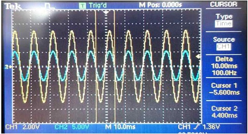
Fig. 19 shows the final result waveform. In the experimental environment, the same data was input to only two channels and operated in continuous mode. At the beginning of the experiment, the signal was distorted after a certain period of time in the data output, but it was identified as a problem with the generation period of the SPI output and was corrected.
Ⅵ. Conclusion
In the existing board, signal distortion occurred when the channel was changed or the data was cut off. In addition, generation of noise was a cause of distortion. To compensate for this, the system was implemented using FPGA, and it can be seen that it operates without unreasonableness even when executed under the same conditions as distortion. Existing boards have the disadvantage of being expensive because they have unnecessary functions in addition to the functions required by the user. When using the method presented in this paper, since only the necessary parts are implemented, it is competitive in price and has the advantage of being able to modify it because it is implemented in FPGA. This method also can be used in the module for viewing results in digital image processing.
Acknowledgments
This research was supported by Kumoh National Institute of Technology(2019-104-015)
References
-
X. F. Zhang and H. X. Luo, "A Multi-Channel Data Acquisition System and its Performance Analysis Method Based on FPGA", Advanced Materials Research, Vol. 490–495, pp. 37–41, Mar. 2012.
[https://doi.org/10.4028/www.scientific.net/AMR.490-495.37]

-
B. Lonla Moffo and J. Mbihi, "A Novel Digital Duty-Cycle Modulation Scheme for FPGA-Based Digital-to-Analog Conversion", IEEE Transactions on Circuits and Systems II: Express Briefs, Vol. 62, No. 6, pp. 543–547, Jun. 2015.
[https://doi.org/10.1109/TCSII.2015.2407233]

-
C. H. Liu, J. S. Ji, and A. Q. Qi, "Design of Control Module for Serial DAC Based on FPGA", Advanced Materials Research, Vol. 765–767, pp. 2456–2459, Sep. 2013.
[https://doi.org/10.4028/www.scientific.net/AMR.765-767.2456]

-
E. Miyata, C. Natsukari, D. Akutsu, T. Kamazuka, M. Nomachi, and M. Ozaki, "Fast and flexible CCD-driver system using fast DAC and FPGA", Nuclear Instruments and Methods in Physics Research Section A: Accelerators, Spectrometers, Detectors and Associated Equipment, Vol. 459, No. 1–2, pp. 157–164, Feb. 2001.
[https://doi.org/10.1016/S0168-9002(00)01015-9]

-
Z. Y. Liu, "One-Bit DAC Application Design in Audio Signal Processing", Advanced Materials Research, Vol. 971–973, pp. 1676–1679, Jun. 2014.
[https://doi.org/10.4028/www.scientific.net/AMR.971-973.1676]

-
Tauzin, G., Cordier, B., Gros, M., Mandrou, P., and Crespin, S., "SPI Calibration", Nuclear Instruments and Methods in Physics Research Section A: Accelerators, Spectrometers, Detectors and Associated Equipment, Vol. 442, No. 1–3, pp. 408–411, Mar. 2000.
[https://doi.org/10.1016/S0168-9002(99)01263-2]

-
L. Xiao, L. Li, W. Nie, X. Xie, and H. Wan, "A digital signal processor-based pulse programmer with performance of run-time information handling for magnetic resonance imaging", Measurement Science and Technology, Vol. 26, No. 6, pp. 065402, Apr. 2015.
[https://doi.org/10.1088/0957-0233/26/6/065402]

-
P. Wang, Y. Zhang, and J. Yang, "Design and Implementation of Modified DDS Based on FPGA", Procedia Computer Science, Vol. 131, pp. 261–266, Apr. 2018.
[https://doi.org/10.1016/j.procs.2018.04.212]

-
H. Kirrmann, "Data Format and Bus Compatibility in Multiprocessors", IEEE Micro, Vol. 3, No. 4, pp. 32–47, Aug. 1983.
[https://doi.org/10.1109/MM.1983.291136]

-
M. Lobelle, "VME bus interfacing: A case study", Interfaces in Computing, Vol. 1, No. 3, pp. 193–210, Aug. 1983.
[https://doi.org/10.1016/0252-7308(83)90001-6]

-
N. B. Ameur, N. Masmoudi, and M. Loulou, "FPGA-Based Design Δ–Σ Audio D/A Converter with a Resolution Clock Generator Enhancement Circuit", Journal of Circuits, Systems and Computers, Vol. 24, No. 03, pp. 1550037, Feb. 2015.
[https://doi.org/10.1142/S0218126615500371]

-
S. Dessai and S. G., "Embedded Hardware Circuit and Software Development of USB based Hardware Accelerator", International Journal of Reconfigurable and Embedded Systems(IJRES), Vol. 7, No. 1, pp. 21, May 2018.
[https://doi.org/10.11591/ijres.v7.i1.pp21-33]

-
S. H. Zhu, "Hardware Implementation Based on FPGA of Interrupt Management in a Real-time Operating System", Information Technology Journal, Vol. 12, No. 5, pp. 943–950, Feb. 2013.
[https://doi.org/10.3923/itj.2013.943.950]

-
S. Attia and V. Betz, "Feel Free to Interrupt", ACM Transactions on Reconfigurable Technology and Systems, Vol. 13, No. 1, pp. 1–27, Feb. 2020.
[https://doi.org/10.1145/3372491]

- Tian, Jinwen, Li, Jingqi, Xu, Hongbo, and Liu, Jian, "System hardware design of video image catching and processing system and its realization based TMS320C6414", Journal of Huazhong University of Science and Technology.Nature science edition, Vol. 33, No.7, pp. 17-19, Jul. 2005.
-
Z. H. Liu, Y. L. Mao, and C. L. Song, "One Kind of Data Acquisition System Used in PC104 Embedded Navigation Computer", Applied Mechanics and Materials, Vol. 347–350, pp. 24–27, Aug. 2013.
[https://doi.org/10.4028/www.scientific.net/AMM.347-350.24]


2019 : M.S degrees in Department of Electrical Engineering, Kumoh National Institute of Technology
Research interests : Digital SoC, Image Processing, Verilog HDL

2020 : B.S degrees in Department of Electrical Engineering, Kumoh National Institute of Technology
Research interests : SoC, Interface, Embedded system

1992: BS degree in School of Electronic Engineering, Kumoh National Institute of Technology
2010 : Ph.D. degree in Dept. of Industrial Management, Kumoh National Institute of Technology
2017 ~ present : Associate Professor in Dept. of IT Convergence, Kumoh National Institute of Tech.
Research interests : Industrial System, 3D Printer

1993 : BS degree in Department of Electronic Engineering, Yonsei University
1999 : Ph.D. degree in Department of Electronic Engineering, Yonsei University
2004 ~ present : Professor in School of Electronic Eng., Kumoh National Institute of Tech.
Research interests : SoC, Vision control, Embedded system, Fast serial interface


