
Design of 92.53-dB SNDR Delta-Sigma Modulator with Optimized Sampling Capacitance for High-Precision Sensor Interfaces
 ; Juncheol Kim*
; Young-Chan Jang*
; Juncheol Kim*
; Young-Chan Jang*
Abstract
This paper presents an optimized sampling capacitor design for a Delta-Sigma Modulator (DSM) tailored for high-precision sensor ADCs. By balancing the trade-off between thermal noise and silicon area, an optimal capacitor value was determined and validated via Cadence Spectre simulations and prototype measurements. The second-order Cascaded-of-Integrators Feedforward (CIFF) DSM employs a 3-bit quantizer, a 512 kHz sampling rate, an oversampling ratio of 512, and a 500 Hz signal bandwidth. Fabricated in a 180 nm CMOS process with a 1.8 V supply, the design utilizes a 1.03 pF sampling capacitor. Measurement results demonstrate a 92.53 dB SNDR for a 100 Hz input, closely matching the 93.81 dB simulation prediction, which confirms the proposed strategy's effectiveness in achieving high-resolution performance with minimized area overhead.
초록
본 논문은 고정밀 센서 ADC에 최적화된 델타-시그마 변조기(DSM)용 샘플링 커패시터 설계를 제시한다. 열 잡음과 실리콘 면적 간의 상충 관계를 균형 있게 고려하여 최적의 커패시터 값을 도출하였으며, Cadence Spectre 시뮬레이션과 시제품 측정을 통해 이를 검증하였다. 2차 캐스케이드 적분기 피드포워드 DSM은 3비트 양자화기, 512 kHz 샘플링 속도, 512의 오버샘플링 비율, 500 Hz 신호 대역폭을 채택한다. 1.8 V 전원을 사용하는 180 nm CMOS 공정으로 제작된 이 설계는 1.03 pF 샘플링 커패시터를 활용한다. 칩 측정 결과, 100 Hz 입력에 대해 92.53 dB의 SNDR을 보여주었으며, 이는 93.81 dB의 시뮬레이션 예측값과 매우 근접하여, 제안된 전략이 면적 오버헤드를 최소화하면서 고해상도 성능을 달성하는 데 효과적임을 입증한다.
Keywords:
delta-sigma modulator, analog-to-digital converter, cascaded-of-integrators feedforward, noise simulation, sampling capacitorⅠ. Introduction
High-resolution Analog-to-Digital Converters (ADCs) serve as a fundamental building block in modern sensor interface applications, including industrial instrumentation, medical diagnostic devices, and environmental monitoring systems [1]-[9]. These applications typically demand a high dynamic range to process low-amplitude signals from sensors, despite operating within a relatively narrow bandwidth. Among various ADC architectures, the Delta-Sigma Modulator (DSM) has emerged as the most viable solution for achieving high Signal-to-Noise-and-Distortion Ratio (SNDR) and superior linearity [10]. Its effectiveness stems from the synergistic combination of oversampling and noise-shaping techniques, which shift quantization noise to higher frequencies, away from the signal band of interest [11][12]. As the demand for higher resolution increases, the design of the first-stage integrator in a DSM becomes increasingly critical. In high-precision designs, the overall performance is primarily limited by thermal noise, specifically the kT/C noise generated during the sampling phase, rather than the quantization noise itself [13]. To achieve a target SNDR, the conventional design approach involves increasing the size of the Sampling Capacitor (CS) to suppress this thermal noise floor. For example, a recent study [1] presented an incremental delta-sigma ADC for sensor Readout Integrated Circuits (ROICs), achieving a remarkable 95.8-dB SNDR through advanced analog noise reduction techniques. However, achieving such high performance often necessitates the use of significantly large sampling capacitors to ensure that the thermal noise power remains well below the signal level. While increasing CS improves noise performance, it introduces significant design trade-offs regarding silicon area and power efficiency [14]. Large capacitors occupy a substantial portion of the chip area, directly increasing the manufacturing cost per die. Furthermore, an increased CS imposes a heavier capacitive load on the Operational Transconductance Amplifier (OTA) within the integrator. To maintain the required unity-gain bandwidth and ensure proper settling within each sampling phase, the OTA must provide a higher transconductance (gm), which inherently leads to increased bias currents and higher total power consumption [15]. Consequently, an oversized sampling capacitor can jeopardize the power- area- performance efficiency that is crucial for battery-powered or multi-channel sensor interfaces [16]. Therefore, a systematic optimization strategy is required to determine the minimum possible sampling capacitance that satisfies the target dynamic performance without unnecessary area overhead. This paper proposes an optimized design methodology for the sampling capacitor in a second-order Cascade of Integrators with Feedforward (CIFF) DSM. By conducting a strategic analysis of the noise-shaping function and the thermal noise contribution specific to the CIFF architecture [11], we derive an optimal CS value that balances the stringent requirements of high-precision sensor interfaces. The proposed DSM, incorporating a 3-bit quantizer and an Oversampling Ratio (OSR) of 512, was designed and fabricated using a 180 nm CMOS process with a 1.8 V supply. Unlike previous works that may rely on excessive design margins, this work utilizes a 1 pF sampling capacitor, determined through rigorous quantitative analysis. The design was validated using Cadence Spectre noise simulations and confirmed through physical measurements of the fabricated chip. The experimental results show an SNDR of 92.53 dB for a 100 Hz input, closely matching the simulated prediction of 93.81 dB. These results demonstrate that the proposed optimization strategy effectively achieves high-resolution performance while minimizing the silicon area and easing the drive requirements of the internal amplifiers.
Ⅱ. Sampling Capacitor for DSM Considering Thermal Noise
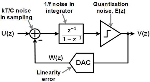
Figure 1 illustrates the fundamental block diagram of a DSM. It primarily consists of a loop filter (Integrator), a quantizer, and a Digital-to-Analog Converter (DAC) in the feedback path to subtract the output from the input signal. Based on the linear model, the modulator output, V(z), is expressed as:
| (1) |
Basic block diagram of the DSM and noise sources in each building block
where U(z) is the input signal, W(z) represents the DAC output signal, and E(z) denotes the quantization noise. As shown in Equation (1), the difference between the input signal and the feedback DAC output is processed through a low-pass characteristic (Signal Transfer Function, STF), whereas the quantization noise, E(z), is subjected to a high-pass characteristic (Noise Transfer Function, NTF). This mechanism, known as noise shaping, effectively shifts the quantization noise power from the low-frequency signal band to higher frequencies. Consequently, the DSM can significantly enhance the signal-to-noise ratio (SNR) within the bandwidth of interest. Furthermore, this architectural advantage can be leveraged alongside an increased Oversampling Ratio (OSR) to achieve even higher dynamic range and superior SNR performance [17].
Despite these advantages of the DSM, various non-idealities inherent in these building blocks can degrade the overall performance; however, several design techniques are implemented to mitigate these effects. Among these, the 1/f noise (flicker noise) originating from the Operational Transconductance Amplifier (OTA) within the integrator, as well as the linearity errors from the feedback DAC, are effectively suppressed using chopping and Dynamic Element Matching (DEM) techniques, respectively [18][19]. Furthermore, the thermal noise (kT/C noise) accumulated during the sampling of the analog input and feedback signals is recognized as an input-referred error. As this noise is processed by the same Signal Transfer Function (STF) as the analog input U(z) and is not suppressed by the Noise Transfer Function (NTF), it establishes a fundamental limit on the achievable Signal-to-Noise Ratio (SNR) and dynamic range[11]. To maintain a high dynamic range and minimize the thermal noise floor, the sampling capacitor (CS) must be sized sufficiently large to meet the required noise specifications. However, the sizing of CS, in conjunction with the feedback capacitor (CI) of the integrator, significantly dictates the total silicon area and power consumption of the DSM[20]. Therefore, these capacitance values must be optimally determined by carefully balancing the trade-off between thermal noise performance, hardware efficiency, and the overall dynamic performance requirements of the modulator [21].
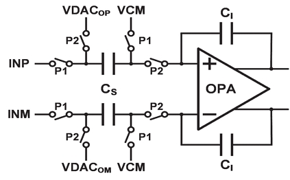
The differential Switched-Capacitor (SC) integrator shown in Fig. 2 operates over two non-overlapping clock phases: the sampling phase (P1) and the integration phase (P2). During P1, the input signal is sampled onto the capacitors CS. Simultaneously, thermal noise from the switches is sampled, contributing a noise power of kT/CS to each sampling capacitor. During the subsequent integration phase (P2), charge transfer occurs from CS to the integration capacitor CI. In this phase, additional thermal noise from the DAC feedback path is accumulated. This process results in a total input-referred noise power of 2kT/CS per side. For a fully differential configuration, the noise contributions from both phases and both paths result in a total input-referred thermal noise power expressed as
| (2) |
Circuit diagram Switched-capacitor integrator
where k is the Boltzmann constant and T is the absolute temperature. This noise power is independent of switch resistance or timing, being fundamentally constrained by the sampling capacitance CS. In high-resolution DSMs, thermal noise often becomes the dominant performance bottleneck. While an ideal DSM is limited only by quantization noise, the kT/C noise floor can degrade the actual SNR significantly[11][22]. To achieve a target resolution, CS must be sized such that the thermal noise remains sufficiently below the quantization noise floor. However, an excessively large CS leads to penalties in silicon area, increased RC delays, and higher power consumption.
The SNR of the DSM is defined by the ratio of the signal power (Psignal) to the total noise power (Pnoise):
| (3) |
For a sinusoidal input with a maximum amplitude of Vp/2, the required total noise power to meet a specific SNR target is:
| (4) |
By incorporating the effects of oversampling, the in-band thermal noise power is reduced by the OSR. The in-band noise Power Spectral Density (PSD) is given by:
| (5) |
By equating the required noise power for the target SNR with the oversampled thermal noise, the minimum required sampling capacitance CS is derived as:
| (6) |
This relationship allows for the optimal selection of the sampling capacitor size based on the target system specifications and the architectural oversampling ratio. For instance, to achieve a target SNR of 93 dB with a 3 dB design margin, the SNR objective is set to 96 dB. Assuming Vp is 1 V, and an OSR of 512, the minimum sampling capacitance CS is determined to be 1.03 pF.
The relationship between the SNR, thermal noise, and sampling capacitance CS shown in Equation (6) was verified through the behavioral simulation of the DSM using MATLAB Simulink. Figure 3(a) illustrates the behavioral model of the second-order CIFF DSM. The architecture incorporates two integration stages (INT1 and INT2) with local feedback gains and a feedforward path to the summation node before quantization. A 3-bit SAR quantizer is employed to convert the analog signal into a digital output. To reflect real-world circuit constraints, a thermal noise block (kT/C noise) is included at the input stage, where the noise level is precisely calculated based on Equation (5) using parameters such as the sampling capacitance, absolute temperature (300 K), and the Boltzmann constant. The dynamic performance of the modulator is analyzed through its Power Spectral Density (PSD) and SNDR characteristics. As shown in Fig. 3(b), in the absence of thermal noise, the modulator exhibits superior dynamic performance with an ideal SNDR of 117.64 dB. However, when thermal noise is considered, the SNDR degrades due to the kT/C noise floor. With a sampling capacitance (CS) of 1 pF and an OSR of 512, the modulator achieves an SNDR of 92.26 dB and an effective number of bits (ENOB) of 15.03 bits for a signal frequency (fsig) of 100 Hz and a sampling frequency (fs) of 512 kHz. Notably, this simulated SNDR of 92.26 dB is consistent with the theoretical value derived from Equation (6), confirming the validity of the noise analysis. Fig. 3.(c) illustrates the dependency of the SNDR on the sampling capacitance (CS). As the capacitance increases from 0.1 pF to 2.2 pF, the SNDR improves from approximately 82 dB to 95 dB. This trend confirms that a larger sampling capacitor reduces the impact of thermal noise (kT/C), thereby enhancing the overall dynamic range of the system.
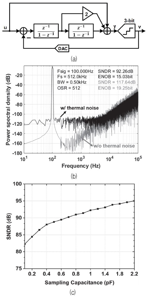
Behavioral simulation of second-order CIFF DSM (a) proposed system block diagram (b) power spectral density with and without thermal noise for CS = 1 pF and OSR = 512 (c) SNDR performance as function of sampling capacitance CS
Ⅲ. Design of Delta-Sigma Modulator with optimized Sampling capacitance
The overall architecture of the proposed second-order CIFF DSM is illustrated in Fig. 4. To achieve a target SNDR of 93 dB for an input signal bandwidth of 500 Hz, the modulator is designed with an OSR of 512, resulting in a sampling frequency (fs) of 512 kHz. Table 1 shows the target specifications for the designed DSM. As shown in Fig. 4(a), the system consists of two fully differential integration stages and a 3-bit SAR ADC that serves as the internal quantizer. The choppers and Data Weighted Averaging (DWA) logic aress incorporated to eliminate the flicker noise of the operational amplifiers in the integrators and the nonlinearity of the 3-bit CDAC, respectively. Figure 4(b) illustrates the detailed timing diagram of the proposed modulator. The system operates with an External Clock (EXCLK) of 3.584 MHz, and one complete conversion cycle of the DSM consists of 512 cycles of EXCLK. During the sampling phase (P1), the input signal is sampled onto the 3-bit CDAC array. This is followed by the SAR Conversion phase (SAR_CONV), where the 3-bit quantizer determines the digital output D[2:0]. Subsequently, the integration phase (P2) is executed to process the residue. To mitigate low-frequency noise and mismatch errors, the CHOPPER and DWA_CLK signals are synchronized with the sampling periods, ensuring that flicker noise and DAC nonlinearity are effectively suppressed throughout the conversion process.
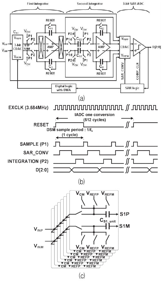
Proposed second-order CIFF DSM (a) entire block diagram (b) timing diagram (c) circuit diagram of 3-bit DAC

Design specifications
Although the proposed architecture is similar to the one reported in [23], it has been specifically designed with an optimized sampling capacitance to achieve the target dynamic range while maintaining a small area for the DSM implementation. The first integrator stage is particularly critical as it directly samples the input signal VINP/M. To satisfy the stringent noise requirements while accounting for thermal noise, the total sampling capacitance at the input stage is optimized based on the analysis in Equation (6). Consequently, the total sampling capacitance CS is set to 1.03 pF. As depicted in Fig. 4(c), this capacitance is realized by the parallel combination of seven CS1 unit capacitors within the 3-bit DAC array, ensuring the thermal noise floor is sufficiently suppressed to maintain the target dynamic performance. Bootstrapped switches are used at the input to prevent harmonic distortion and ensure complete settling of the 1.03 pF sampling capacitor.
Figure 5 shows the block diagram of the reference driver designed to provide stable reference voltages (VREFP, VCM, and VREFM). It incorporates a Bandgap Reference (BGR) to generate a stable 0.8 V source, followed by a Low-Dropout (LDO) regulator and a driver buffer to supply 1.4 V, 0.9 V, and 0.4 V, respectively, ensuring reliable operation of the SAR quantizer.
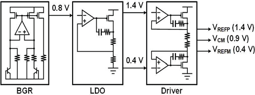
Block diagram of reference driver
To achieve the target performance of a DSM, a practical capacitor sizing methodology is required. While theoretical interpretations provide a fundamental basis, design engineers must account for the specific operational characteristics of SPICE-level simulation tools like Cadence Spectre. Unlike theoretical models, these simulators solve system equations (e.g., KCL) based on device-level models. Therefore, to accurately reflect noise behavior in Switched-Capacitor (SC) circuits, the noise folding effects during the sampling process must be fully integrated into the simulation setup. In practical noise simulations, integrating noise power up to infinite frequencies is not feasible. Thus, the selection of the maximum noise frequency bandwidth (fmax) is critical. As shown in (7), fmax is defined as a multiple of the sampling frequency (fs):
| (7) |
where Nmsb is the parameter determining the frequency range for noise verification. Setting fmax excessively high leads to inefficient simulation times, whereas an insufficient fmax results in an underestimation of the sampled noise. The thermal noise power integrated up to fmax is expressed as:
| (8) |
To evaluate the coverage of the simulation bandwidth relative to the actual circuit bandwidth, a normalization index Fnorm is introduced:
| (9) |
The noise error (ε), representing the difference between the finite integrated noise and the total theoretical noise (√(kT/C)), is derived as:
| (10) |
The relative error rate (E) is expressed in percentage form:
| (11) |
By establishing the relationship between the switch-on duration (Tp = α·τ) and the clock cycle (1/fc = Tc = Np·Tp), the value of Nmsb can be systematically determined based on the target error rate E and the time constant factor α. In this work, to maintain a noise error rate of approximately 1%, fmax was set to 50 times the sampling frequency (fmax = 50·fc) [24].
Figure 6 presents the PSD of the proposed second-order CIFF DSM, simulated using Cadence Spectre. To verify the design’s robustness and the accuracy of the noise modeling, the simulation was conducted under two distinct conditions: without transient noise (Fig. 6(a)) and with transient noise enabled (Fig. 6(b)). The PSD analysis was performed with a signal frequency (fsig) of 100 Hz and a sampling frequency (fs) of 512 kHz, maintaining an OSR of 512. In the absence of transient noise (Fig. 6(a)), the modulator achieves an ideal SNDR of 114.57 dB and an ENOB of 18.74 bits, representing the quantization noise floor limited by the circuit architecture. For the transient noise simulation in Fig. 6(b), the maximum noise frequency (fmax) was set to 25.6 MHz, which is 50 times the sampling frequency (50·fs), as derived in the methodology section. This ensures that the noise folding effects are accurately captured while maintaining simulation efficiency. Under this condition, the modulator achieves an SNDR of 93.81 dB and an ENOB of 15.29 bits, effectively reaching the design targets. This result exhibits a high degree of correlation with the behavioral simulation results shown in Fig. 3(c). Such close agreement indicates that the transient noise simulation, configured with the optimized fmax, reliably reflects the practical circuit performance, including the thermal noise-dominated noise floor and the characteristic 40 dB/dec noise-shaping slope. This validates both the proposed design methodology and the accuracy of the sampling capacitance optimization.
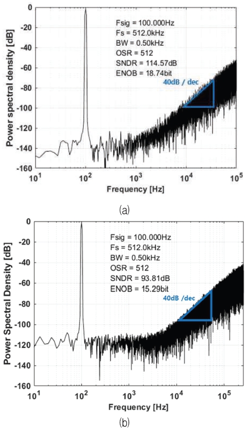
Simulation results of proposed second-order CIFF DSM using Cadence Spectre (a) w/o noise (b) w/ noise
Ⅳ. Chip Implement and measurement results
The proposed second-order CIFF DSM, along with an integrated reference driver, was fabricated using a 180-nm CMOS process with a 1.8-V supply voltage, as shown in Fig. 7(a). In applications involving low-speed sensors and high-voltage circuits, the 180-nm CMOS process is still used for mass production. The sampling frequency of the proposed second-order CIFF DSM is 512 kHz to implement an input bandwidth of 500 Hz and an oversampling ratio of 512. To implement this, the EX_CLK signal with a frequency of 3.584 MHz is fed to the implemented second-order CIFF DSM. The power consumption of the proposed second-order CIFF DSM is 112.8 μW. Fig. 7(b) presents a detailed view of the chip photograph, specifically highlighting the proposed second-order CIFF DSM. The active area of the DSM core is 0.184 mm2.
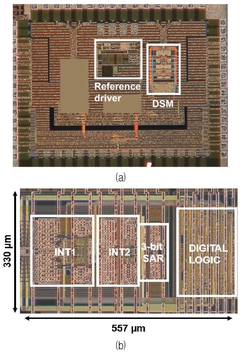
Photograph of fabricated 2nd-order CIFF DSM (a) chip including reference driver (b) 2nd-order CIFF DSM
The first integrator (INT1) occupies 0.02656 mm², the largest area among the analog blocks. The second integrator (INT2) and the 3-bit SAR quantizer occupy 0.0165 mm² and 0.00698 mm², respectively. The digital logic occupies 0.03306 mm². By employing a small sampling capacitor of 1.03 pF, the integration capacitor of the first integrator was proportionally scaled down. This reduction contributed to a decrease in the active area of the first integrator compared to the design in [1]. The capacitors used in the proposed second-order CIFF DSM, including the 3-bit capacitor array of the first integrator, were implemented using Metal-Insulator-Metal (MIM) capacitors as unit capacitors. A unit MIM capacitor with dimensions of 4.35 μm × 8 μm is utilized for the sampling capacitor, providing a unit capacitance of 71.3 fF.
The measured dynamic performance of the fabricated second-order CIFF DSM is illustrated in Fig. 8. The PSD was measured under the same conditions as the simulations: a signal frequency (fsig) of 100 Hz and a sampling frequency (fs) of 512 kHz with an OSR of 512. The measured SNDR and ENOB are 92.53 dB and 15.08 bits, respectively. Notably, these measurement results exhibit a high degree of consistency with both the behavioral simulation (Fig. 3(c)) and the Cadence Spectre transient noise simulation (Fig. 6(b)), where the latter was configured with fmax = 50·fs. The measured noise floor accurately reflects the optimized thermal noise levels, and the second-order noise-shaping characteristic of 40 dB/dec is clearly maintained in the higher frequency range. This close correlation across behavioral modeling, circuit-level simulation, and silicon measurement validates the reliability of the proposed practical capacitor sizing methodology and confirms that the transient noise simulation effectively predicts real-world performance.
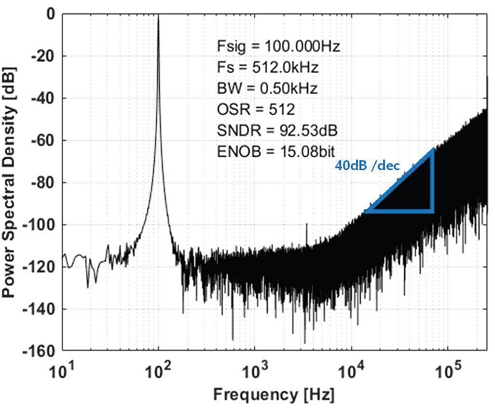
Measured dynamic performances of 2nd-order CIFF DSM
Table 2 provides a comprehensive performance comparison between this work and previously reported DSMs. Fabricated in a 180-nm CMOS process, the proposed DSM achieves a competitive SNDR of 92.5 dB while maintaining a compact active area of 0.184 mm².
Performance comparison of DSMs
Compared to other designs implemented in the same 180-nm technology node, such as [25],[26] and [1], this work demonstrates a superior balance between high-resolution performance and silicon area. Specifically, while [26], [29] and [1] report higher or similar SNDR, they occupy substantially larger areas of 0.8 mm² and 0.245 mm², respectively. The achievement of a high SNDR with a minimized area overhead is primarily attributed to the systematic determination of the sampling capacitor (CS = 1.03 pF), which allowed for the proportional scaling of the subsequent integration capacitors. Consequently, the proposed design offers a highly area-efficient solution for high-precision sensor interface applications without compromising dynamic range or noise performance.
Ⅴ. Conclusion
This paper presented a practical and optimized design methodology for determining the sampling capacitor size in a high-precision DSM. Through a comprehensive quantitative analysis of the trade-off between dynamic performance and silicon area, an optimal sampling capacitance of 1.03 pF was established for the proposed second-order CIFF architecture. This optimization not only ensured superior noise performance but also enabled a significant reduction in the overall silicon area by scaling down the integration capacitors proportionally. The validity of the proposed methodology was rigorously verified through a multi-stage verification process. The behavioral simulation, Cadence Spectre transient noise simulation which is configured with an optimized noise bandwidth (fmax = 50·fs), and experimental measurements of the fabricated prototype showed a high degree of correlation. Specifically, the measured SNDR of 92.53 dB closely matched the transient noise simulation result of 93.81 dB, confirming that the simulation environment effectively predicts real-world hardware performance. Fabricated in a 180-nm CMOS process, the prototype successfully achieved high-resolution performance with minimized area overhead. These results demonstrate that the proposed sizing strategy is a highly effective approach for design engineers to achieve target DSM specifications while optimizing for area efficiency in sensor interface applications.
Acknowledgments
This research was supported by the ITRC support programs (IITP-2026-RS-2024-00438288) through the IITP funded by the MSIT and the Basic Science Research Program (2018R1A6A1A03024003) through the NRF funded by the Ministry of Education, Republic of Korea. The EDA tool was supported by the IC Design Education Center, Republic of Korea.
References
-
J. Kim and Y.-C. Jang, "A 1.8-V 95.8-dB SNDR Incremental Delta-sigma ADC with Analog Noise Reduction Techniques for Sensor ROIC", IEEE Access, Vol. 13, pp. 114256-114267, Jun. 2025.
[https://doi.org/10.1109/ACCESS.2025.3583830]

-
V. Quiquempoix, P. Deval, A. Barreto, G. Bellini, J. Markus, and J. Silva., "A low-power 22-bit incremental ADC", IEEE J. Solid-State Circuits, Vol. 41, No. 7, pp. 1562–1571, Jul. 2006.
[https://doi.org/10.1109/JSSC.2006.873891]
-
C. Chen, Z. Tan, and M. A. P. Pertijs, "A 1 V 14 b self-timed zerocrossing-based incremental ADC", IEEE Int. Solid-State Circuits Conf. (ISSCC) Dig. Tech. Papers, San Francisco, CA, USA, pp. 274-275, Feb. 2013.
[https://doi.org/10.1109/ISSCC.2013.6487732]
-
A. Agah, K. Vleugels, P. B. Griffin, M. Ronaghi, J. D. Plummer, and B. A. Wooley, "A high-resolution low-power oversampling ADC with extended-range for bio-sensor arrays", IEEE J. Solid State Circuits, Vol. 45, No. 6, pp. 1099-1110, Jun. 2010.
[https://doi.org/10.1109/JSSC.2010.2048493]
-
J. Kim, W. Jung, S. Lim, Y. Park, Wo. Choi, and Y. Kim, "A 14 b extended counting ADC implemented in a 24Mpixel APS-C CMOS image sensor", IEEE Int. Solid-State Circuits Conf. (ISSCC) Dig. Tech. Papers, San Francisco, CA, USA, pp. 390-392, Feb. 2012.
[https://doi.org/10.1109/ISSCC.2012.6177060]
-
C.-H. Chen, J. Crop, J. Chae, P. Chiang, and G. C. Temes, "A 12-bit 7 μW/channel 1 kHz/channel incremental ADC for biosensor interface circuits", Proc. IEEE Int. Symp. Circuits Syst. (ISCAS), Seoul, South Korea, pp. 2969-2972, May 2012.
[https://doi.org/10.1109/ISCAS.2012.6271940]
-
Y. Zhang, C.-H. Chen, T. He, and G. C. Temes, "A 16 b multistep incremental analog-to-digital converter with single-opamp multi-slope extended counting", IEEE J. Solid-State Circuits, Vol. 52, No. 4, pp. 1066-1076, Apr. 2017.
[https://doi.org/10.1109/JSSC.2016.2641466]
-
Y. Chae, K. Souri, and K. A. A. Makinwa, "A 6.3 µW 20 bit Incremental Zoom-ADC with 6 ppm INL and 1 µV Offset", IEEE Journal of Solid-State Circuits, Vol. 48, No. 12, pp. 3019-3027, Dec. 2013.
[https://doi.org/10.1109/JSSC.2013.2278737]
-
Z. Deng, R. Chen, D. Lin, Z. Wu, B. Li, and M. Zhao, "A 4.5 mW 58.7 dB SNDR discrete-time delta–sigma modulator based on MOTFTs for ECG signal recording", Microelectronics Journal, Vol. 166, At. no. 106877, Dec. 2025.
[https://doi.org/10.1016/j.mejo.2025.106877]
-
F. Wang, Y. Tang, and C. Wei, "A discrete-time delta-sigma modulator using adaptive noise shaping enhancement technique", Microelectronics Journal, Vol. 168, Art. no. 106986, Feb. 2026.
[https://doi.org/10.1016/j.mejo.2025.106986]
- S. Pavan, G. C. Temes, and R. Schreier, "Understanding Delta-Sigma Data Converters", Second ed. Hoboken, NJ, USA: Wiley, Mar. 2017.
-
C. Wei, R. Wei, L. Huang, G. Huang, J. Lai, and Z. Tan, "A 1.2 V 2.3 µW 94.7 dB DR Delta-Sigma Modulator With Dynamic-Range Enhancement and Tri-Level CDAC", 2023 IEEE Asian Solid-State Circuits Conference (A-SSCC), Haikou, China, pp. 1-3, Nov. 2023.
[https://doi.org/10.1109/A-SSCC58667.2023.10348006]
-
Z. Wang, B. Li, J. Tang, Z. Wu, H. Luo, Y. Wang, and X. Tang, "A 184.8dB-FoMs 1.6MS/s Incremental Noise-Shaping Pipeline ADC with Single-Amplification-Based kT/C Noise Cancellation Technique", 2025 IEEE International Solid-State Circuits Conference (ISSCC), San Francisco, CA, USA, pp. 1-3, Feb. 2025.
[https://doi.org/10.1109/ISSCC49661.2025.10904507]
- B. Razavi, "Design of Analog CMOS Integrated Circuits", McGraw-Hill, 2016.
-
R. Wei, Z. Zheng, Y. Lin, N. Xu, G. Zhao, and Q. Chen, "Fully dynamic zoom ADC with energy-efficient residue feedforward and two-step summation", Microelectronics Journal, Vol. 154, Art. no. 106474, Dec. 2024.
[https://doi.org/10.1016/j.mejo.2024.106474]
-
J. Silva, U. Moon, J. Steensgaard, and G. C. Temes, "Wideband low-distortion delta-sigma ADC topology", Electronics Letters, Vol. 37, No. 12, Jun. 2001.
[https://doi.org/10.1049/el:20010542]
-
J. M. de la Rosa, "Sigma-Delta Modulators: Tutorial Overview, Design Guide, and State-of-the-Art Survey", IEEE Transactions on Circuits and Systems I: Regular Papers, Vol. 58, No. 1, pp. 1-21, Jan. 2011.
[https://doi.org/10.1109/TCSI.2010.2097652]
-
C. Xing, Y. Zhong, N. Sun, and L. Jie, "A 0.021mm2 92dB-SNDR 88kHz-BW Incremental Zoom ADC with 2nd-order RT-DEM and Quiet Chopping", ESSCIRC 2023- IEEE 49th European Solid State Circuits Conference (ESSCIRC), Lisbon, Portugal, pp. 293-296, Sep. 2023.
[https://doi.org/10.1109/ESSCIRC59616.2023.10268741]
-
S. Mondal, O. Ghadami, and D. A. Hall, "10.2 A 139 µ W 104.8dB-DR 24kHz-BW CT ΔΣM with Chopped AC-Coupled OTA-Stacking and FIR DACs", 2021 IEEE International Solid-State Circuits Conference (ISSCC), San Francisco, CA, USA, pp. 166-168, Feb. 2021.
[https://doi.org/10.1109/ISSCC42613.2021.9366002]
-
T. -C. Wang, Y. -H. Lin, and C. -C. Liu, "A 0.022mm2 98.5dB SNDR hybrid audio delta-sigma modulator with digital ELD compensation in 28nm CMOS", 2014 IEEE Asian Solid-State Circuits Conference (A-SSCC), KaoHsiung, Taiwan, pp. 317-320, Nov. 2014.
[https://doi.org/10.1109/ASSCC.2014.7008924]
-
J. Myung, G. Yun, H. Choee, Y. Kim, S. Ha, and M. Je, "A 99.8-nV/√Hz ΔΣ Modulator with an Input-Impedance-Boosted kT/C-Noise-Cancellation Integrator for Biopotential-Signal Acquisition", 2025 IEEE International Symposium on Circuits and Systems (ISCAS), London, United Kingdom, pp. 1-5, May 2025.
[https://doi.org/10.1109/ISCAS56072.2025.11043192]
-
R. Schreier, J. Silva, J. Steensgaard, and G. C. Temes, "Design-oriented estimation of thermal noise in switched-capacitor circuits", IEEE Transactions on Circuits and Systems I: Regular Papers, Vol. 52, No. 11, pp. 2358-2368, Nov. 2005.
[https://doi.org/10.1109/TCSI.2005.853909]
- N. Jeon, "Incremental Delta-sigma ADC with Rail-to-rail Input Range", M.S. thesis, Dept. of Electronic Engineering, Kumoh National Institute of Technology, Gumi, South Korea, 2023.
- K. Kundert, "Simulating switched-capacitor filters with Spectre RF", www.designers-guide.org/Analysis, . [accessed: Sep. 19, 2025]
-
M. Zhao, Y. Zhao, H. Zhang, Y. Hu, Y. Bao, L. Ye, W. Qu, and Z. Tan, "A 4-μW Bandwidth/Power Scalable Delta–Sigma Modulator Based on Swing-Enhanced Floating Inverter Amplifiers", IEEE J. Solid-State Circuits, Vol. 57, No. 3, pp. 709-718, Mar. 2022.
[https://doi.org/10.1109/JSSC.2021.3123261]
-
Y.-H. Moon, K.-W. Park, K. Kim, M. Kwon, M.-J. Seo, and S.-T. Ryu, "A 250kHz-BW 86.2dB-SNDR 176.7dB-FoMS Fully Dynamic kT/C Noise-Canceled DT DSM with SAR-Assisted Input FF and DNC", 2025 IEEE Asian Solid-State Circuits Conference (A-SSCC), Daejeon, Korea, pp. 304-306, Nov. 2025.
[https://doi.org/10.1109/A-SSCC67472.2025.11349367]
-
A. Boni, L. Giuffredi, G. Pietrini, M. Ronchi, and M. Caselli, "A Low-Power Sigma-Delta Modulator for Healthcare and Medical Diagnostic Applications", IEEE Transactions on Circuits and Systems I: Regular Papers, Vol. 69, No. 1, pp. 207-219, Jan. 2022.
[https://doi.org/10.1109/TCSI.2021.3112342]
-
G. Huang, C. Wei, and Ro. Wei, "A 94.5-dB SNDR 96.5-dB DR discrete-time delta-sigma modulator using FIA assisted OTA and FIR DAC feedback", Microelectronics Journal, Vol. 150, Art. no. 106278, Aug. 2024.
[https://doi.org/10.1016/j.mejo.2024.106278]
-
C. Wei, C. Chen, G. Huang, L. Huang, R. Wang, and R. Wei, "A 1.8 V 98.6 dB SNDR discrete-time CMOS delta-sigma ADC", Microelectronics Journal, Vol. 144, Art. no. 106069, Feb. 2024.
[https://doi.org/10.1016/j.mejo.2023.106069]

2025. 8 : B.S. degree, Dept. of Electronic Engineering, Kumoh National Institute of Technology, South Korea
2025. 8 ~ present : M.S. candidate, Dept. of Semiconductor System Engineering, Kumoh National Institute of Technology, South Korea
Research interests : analog and mixed-signal IC design, with an emphasis on high-resolution and noise-shaping ADCs for precision sensor interfaces

2022. 2 : B.S. degree, Dept. of Electronic Engineering, Kumoh National Institute of Technology, South Korea
2025. 2 : M.S. degree, Dept. of Electronic Engineering, Kumoh National Institute of Technology, South Korea
2025. 2 ~ present : Ph.D. candidate, Dept. of Semiconductor System Engineering, Kumoh National Institute of Technology, South Korea
Research interests : analog and mixed-signal circuit design including high-resolution data converters
1999. 2 : B.S. degree, Electronic Engineering, Kyungpook National University, South Korea
2001. 2 : M.S. degree, Electrical and Electronic Engineering, Pohang University of Science and Technology, South Korea
2005. 2 : Ph.D. degree, Electrical and Electronic Engineering, Pohang University of Science and Technology, South Korea
2005. 3 ~ 2009. 8 : Senior Engineer with the Memory Division, Samsung Electronics, South Korea
2009. 9 ~ present : Faculty of the School of Electronic Engineering, Kumoh National Institute of Technology, South Korea
Research interests : high-performance mixed-mode circuit design for VLSI systems such as signaling, clock generation, and analog-to-digital conversion