Design of Interface IP for Automotive I/O Control on SoC FPGA
Abstract
In order to control various input/output devices of automobiles, we simultaneously design interface IP H/W and driving S/W on Zynq SoC FPGA, which combines MCU and FPGA, to be advantageous in terms of noise, heat generation, and speed. To control analog and digital input/output data for automobile control at high speed, each of ADC, DAC, and DI/O is made into IP, and the user controls it using ARM programming through AXI bus. For verification, the chips mounted on the control board were modeled and the designed IP was connected and simulated. After connecting the control board and the Zynq board together, the desired operation was ensured by checking the register map of the PS area and measuring the actual waveform using an oscilloscope. It was confirmed that the maximum error rate between the input ADC data and the calculated data was 0 to 0.65 percent depending on the voltage level. The DAC's output data showed that most signals met the standard level of output, and at high voltage levels, an error rate of up to 1.67% was observed.
초록
자동차의 다양한 입출력 장치의 제어를 위하여 본 논문에서는 MCU와 FPGA가 결합된 Zynq SoC FPGA에 인터페이스 IP H/W와 구동 S/W를 동시 설계하여 잡음, 발열, 속도에 유리하도록 한다. 자동차 제어용 아날로그 및 디지털 입출력 데이터를 고속으로 제어하기 위하여 ADC, DAC, DI/O 각각을 IP화 하고, 사용자는 ARM에서 AXI를 사용하여 제어하도록 한다. 검증을 위해 보드에 장착된 IC를 모델링하고 설계된 IP를 연결하여 시뮬레이션하며, 제어 보드와 Zynq 보드를 연결 후 PS 영역의 레지스터맵 확인 및 오실로스코프를 사용한 파형 측정을 통하여 원하는 동작을 하는지 확인하였다. 입력된 ADC 데이터와 계산된 데이터의 오차율이 최대는 전압 레벨에 따라 0~0.65%의 오차율을 가짐을 확인하였다. DAC의 출력 데이터는 대부분 신호는 기준 신호와 출력 레벨을 보였으며, 높은 전압 레벨에서는 최대 1.67%의 오차율을 보였다.
Keywords:
automobiles, ADC, DAC, interface IP, SoC, FPGAⅠ. Introduction
As the automotive industry accelerates, systems containing sensors combined with user safety and convenience are increasing. Many sensors are used in cars, and they are used to control wheels, audio, speaker and lamps. Sensors in automobiles are applied in many applications and are divided into parts such as engine and transmission, indoor environment, external communication, safety, convenience, and eco-friendliness. In the engine and transmission, engine pressure, vehicle flow rate, acceleration for driving, gyro, and steering angle sensors are used, and in the indoor environment, sensors are used to check internal temperature and humidity, gas sensors, and air quality. Cars use satellite communication devices such as GPS and navigation to communicate with the outside world. For driver safety and convenience, there are image sensors used in around view and rear cameras, collision prevention sensors for distance control, ultrasonic sensors, radar sensors using lasers, airbag operation sensors, sensors that detect external illumination, and infrared sensors. The sensors for eco-friendly factors include exhaust gas and smoke detection.
The data coming from these sensors are analog data, and are input into the car's system and converted into digital data through Analog-to-Digital Converter(ADC)[1]. The data converted to digital is used to control output modules such as lamps, motors, etc. of the vehicle. The output data require not only digital output but also analog output. This is output through a Digital-to-Analog Converter(DAC), and representative examples are car audio and AC motors.
In this paper, the ADC and DAC interfaces used to input and output data from various sensors and the output terminals used in automobiles are designed on FPGA[2] and made into Intellectual Property(IP) and verified. In addition, a self-test IP is designed to check whether the IP is operating normally, and an IP that is used as a digital input/output terminal for digital data that does not go through ADC and DAC is additionally designed and verified.
Ⅱ. Related work
2.1 ADC modeling
Before modeling the ADC, an Integrated Circuit(IC) is selected and used, and the IC used in this paper is LTC2328. Modeling is performed according to the characteristics of the relevant IC. There is a CNV signal to start ADC operation and a BUSY signal to confirm ADC operation[3]. The input ADC data is 16 bits and operates in accordance with the SCK clock. ADC data is transmitted through Serial Peripheral Interface(SPI). Modeling should be designed to fit the range of maximum and minimum timing values by referring to the data sheet. Check whether the input analog data is linearly converted to digital data by referring to the transfer characteristics. The input voltage range is -10.24 to 10.24V, and the data bits are linear to the applied voltage.
2.2 DAC modeling
The LTC2664 IC is used for DAC modeling. It has four DAC channels, and DAC modeling must also be designed to fall within the timing range by referring to the data sheet. The DAC data output through SPI communication is a total of 24 bits, as shown in Table 1, and consists of 4 command code bits, 4 DAC channel address bits, and 16 data bits.
2.3 Verification using Zynq
Zynq is a chip that combines an ARM Cortex-A9 processor based on Xilinx 7-series FPGA architecture and FPGA logic fabric. It is widely used in systems that combine FPGA and ARM, and has the advantage of being able to be verified by constructing the Programmable Logic(PL) area and Processing System(PS) area separately. It is a multi-channel bus called Advanced eXtensible Interface(AXI), enabling data communication between PS and PL areas using a bus optimized for read and write[4][5].
Ⅲ. System structure
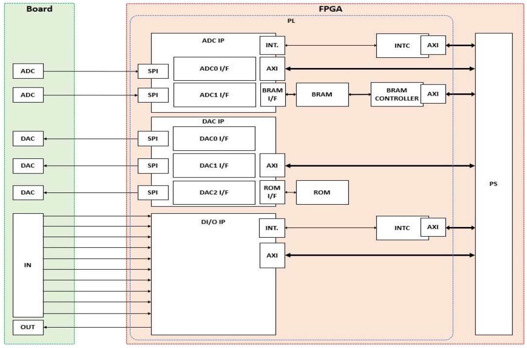
The overall system structure is shown in Fig. 1. The entire system consists of ADC, DAC, and (Digital Input Output)DI/O IP. The protocol of the IP is set through AXI. ADC and DAC IP allow reading and writing data to the corresponding IC through SPI. ADC IP consists of two ADC interfaces and is stored in Block RAM(BRAM) input from each ADC IC, and this data can be read and write through AXI. DAC IP consists of three DAC interfaces and has a structure that loads stored data from ROM and exports it to the DAC IC. Three DAC ICs are used, and each IC has four channels. Therefore, output can be controlled for a total of 12 channels. The DI/O IP consists of 10 inputs and 1 output, and 2 of the 10 inputs are designed to count cumulatively for the time they are pressed, considering that the mode changes depending on the time the button is pressed. PL area design is carried out in Vivado and consists of Verilog-HDL[6]. For the design of the PS area, code is written using C language in Vitis[7], and the PL area and PS area are linked and verified through Zynq[8][9].
Ⅳ. IP design
A total of 4 IPs are used in this system. These are ADC and DAC IPs for input/output conversion data, and DI/O IPs for digital control of external data. Additionally, there is a self-test IP to verify that the ADC and DAC IP are operating normally. Each has its own IP protocol and is controlled through AXI. The size of the data bit is 32 bits.
4.1 ADC IP
As seen in the overall system structure in Fig. 1, ADC IP has two interfaces[10], ADC0 and ADC1, and has a protocol as shown in the Table 2 to control them through AXI. The interrupt is recognized by the PS as a signal that reading and storing data has been completed. The run mode is determined depending on the protocol settings, and there are a method to read and save data only once and a method to read and save data 1,000 times. The data has a size of 16 bits, and dual port RAM is used to store it. When reading from the ADC only once, the data is stored at address 0, and when new data is applied, address 0 is overwritten. Depending on the setting mode, when data 1,000 is read and saved from the ADC, the data is stored in addresses 0 to 999. Since the stored data is read in 32-bit size through AXI, taking this into account, the two data are combined and stored as one data. Once the storage cycle for each execution mode is complete, it terminates by writing a '1' to the COMPLETE bit of the protocol.
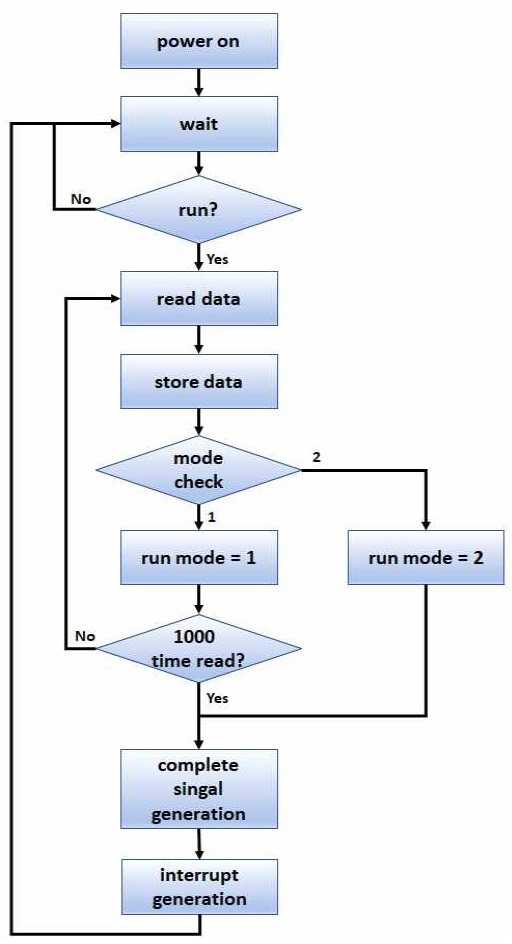
Fig. 2 shows the flowchart of ADC operation. When power is applied and the RUN signal is applied through AXI, the data read from the ADC is read and stored. At this time, check whether the run mode is 1 or 1,000, and if the mode is 1, repeat this 1,000 times. When the process of saving data read from the ADC is completed 1,000 times, or when the mode is 2 and data storage is completed, ‘1’ is written to the complete bit of the corresponding ADC defined in the register map and an interrupt is generated.
The interrupt is checked in the PS area, the complete bit of the corresponding ADC is initialized to '0', and the interrupt is cleared. Additionally, the data is specified as a parameter so that the user can control the number of 1,000 occurrences of data in the IP.
4.2 DAC IP
In the case of DAC IP, IP is used in audio, speakers, etc. used in the vehicle's analog output. As shown in Fig. 1, DAC IP has three DAC interfaces[11], and each interface transmits data to the DAC IC through SPI. The DAC IC used in this paper has four channels, and the sequence is configured to sequentially update data on channels 0 to 3. The data has a structure in which it is loaded and transmitted from BRAM.
Table 3 shows the protocol of DAC IP. The first address contains 16-bit data for self-test in the upper bit, and determines whether to export self-test data or data suitable for the DAC mode depending on the operating mode. In DAC mode, there are different types of amplitude, phase, and frequency required in the output analog waveform. Once the desired mode is determined, the data starting point, frequency, and amplitude appropriate for the output are determined, and data is loaded from BRAM according to the corresponding values. BRAM contains all data and has a structure that loads by setting address values according to the situation. The second to fourth addresses in Table 3 are used to output the temperature and air quality used outside and inside the vehicle. Data is written to the lower 16 bits, and is output consistently when a value is written to the 16th bit.
Fig. 3 shows the DAC flowchart. The mode is selected and the self-test is checked. If it is not in the self-test mode, data is exported according to the mode, and after outputting the 0th channel, change the DAC channel command in Table 1 and output to the next channel. This sequence is output to all four channels and then ends. The output of each channel can be set to be the same, and different outputs are also possible. If it is the self-test, print the data in the self-test and check it in the self-test mode.
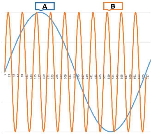
Fig. 4 shows a portion of the output by DAC mode. The IP is designed to change the way the data address value is read depending on the setting mode, and the frequency changes accordingly.
4.3 DI/O IP
DI/O IP is used to control the digital input and output of the vehicle. This includes vehicle lamps, display output, vehicle buttons, etc. As shown in Fig. 1, the IP is consisted an IP with 10 input buttons and only 1 output. Considering that the vehicle's input button is turned on/off by pressing, there are 8 general input buttons, and there are cases where certain buttons, such as the air purification mode, change the mode depending on the time the button is pressed. Therefore, the two digital input buttons are designed to count data for the time they are pressed. Table 4 shows the DI/O protocol. The first address is largely composed of three parts. Among the 10 inputs, it is divided into an input part that indicates the input state that does not use counting, an output part that activates data output, and an interrupt part that occurs when the input changes. In the case of the interrupt part, the posedge, negedge of the 8 input buttons, and negedge of the count input are checked, and when an interrupt occurs, the corresponding bit is set to 1.
Fig. 5 shows an example of an interrupt occurring when a digital input is applied.
In this timing diagram, In1, In2, and In3 represent typical inputs, and In9 represents the count input. An interrupt occurs when the general input is turned on and off, and the count input occurs only once when the count value is saved when the count input is turned off. A total of 10 interrupt signals are delivered to the PS as one interrupt output signal through OR operation.
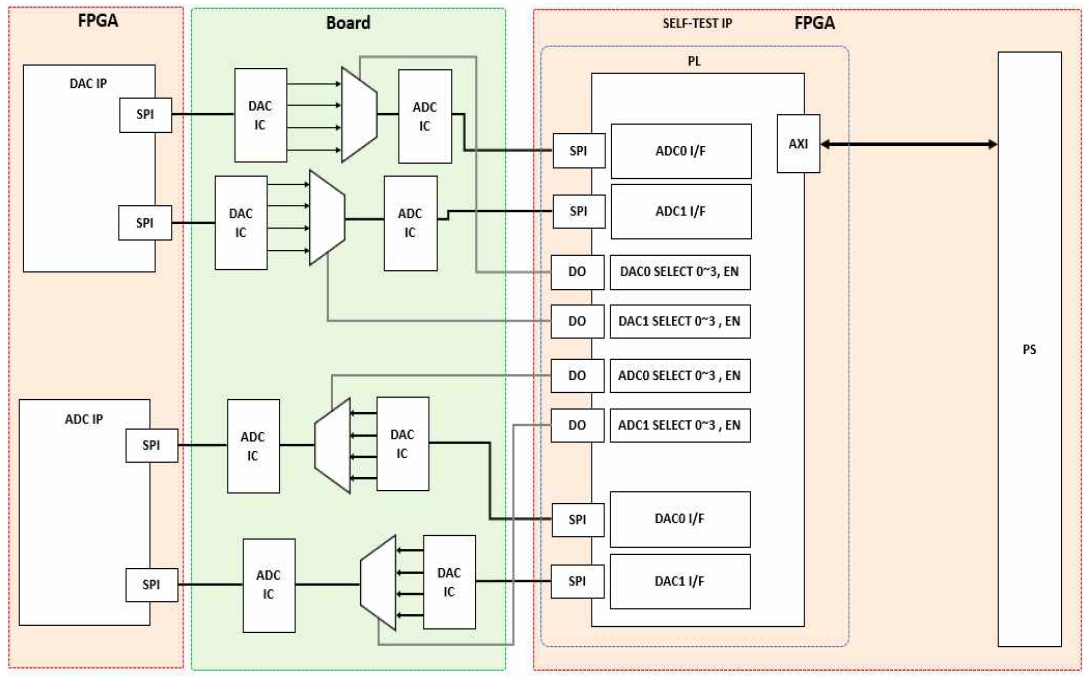
4.4 Self-test IP
The self-test IP is an IP used to check whether the functions of the DAC and ADC IP mentioned in the previous system are operating properly and has the structure shown in Fig. 6. Two ADC interfaces are recycled and configured, and two DAC interfaces are newly configured to check operation. Data is transmitted through SPI, like existing ADC and DAC. The self-test IP is used to verify the mode using the protocol. The protocol is shown in Table 5. Two addresses represent the operation and data of DAC0 and DAC1, and the other two addresses represent the data, execution, and completion of ADC0 and ADC1. One address value represents digital data output. Using the 20 ports of this IP's data output, the enable signal and select signal are determined for the four mux. Data output from the existing DAC IP is transmitted to the DAC IC, and the four channel data output from the IC is applied to the mux. Data that has passed through the mux is input to the ADC IC through the data output of the self-test. The data is read by the self-test ADC IF, and the data stored in the registry map is compared with the data written by the DAC to check whether the correct data has been transmitted.
In the opposite case, if you extend the data to the DAC interface of the self-test and output it through the run bit, the data will be transmitted to the DAC IC through SPI. The IC's channel output is linked to MUX, and the data received from the ADC IP is checked.
Ⅴ. FPGA implementation and verification
The zybo z7-20 board and Vivado 2023.1 version were used for FPGA verification. It was verified using the push button, toggle switch, and Pmod port of the zybo z7-20 board, and the output was verified using LED. The DI/O IP checked the interrupt generated by the change of the input switch in the PS area and confirmed it by reading the corresponding register value. The code was written to clear immediately when an interrupt occurs.
5.1 Verification of ADC IP
To verify ADC IP, voltage is applied to the ADC IC using a power supply, and the output digital value is confirmed through PS. In order to check the precision, the data is judged by looking at the output digital value as the average value once and 1,000 times. Table 6 shows the read data values, which are graphed in Fig. 7. It can be seen that the data increases linearly, and the data for one operation and the average data for 1,000 operations have similar values. The voltage used in the IC is 0 to 10.24 volts, and when a voltage of 10.5 volts was applied, it was confirmed that the maximum value of 32,767 was obtained in two tests.
5.2 Verification of DAC IP
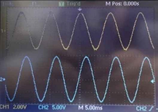
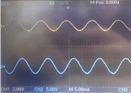
Data read from Zynq's BRAM is passed to the DAC IC, which transmits SPI communication. The transmitted data is output through the IC, and the output waveform of each mode is checked using an oscilloscope. Fig. 8 shows part of the waveform of mode 1. Shows the output waveforms of two different phases. Here, the vertical sensitivity of channel 1 is 2V, and the vertical sensitivity of channel 2 is 5V. Fig. 9 shows the output waveform of mode 2, showing a waveform with different amplitude and phase than Fig. 8. Table 7 displays values for the DAC output waveform. The reference phase is 0 degrees, and the phase is output differently depending on the mode selection value, confirming normal operation.
Ⅵ. Conclusion
We designed DAC, ADC, and DIO IP used in automotive systems so that they can be used according to the situation. The FPGA used was the Zynq series, and when a start/stop signal is sent from the PS area based on the given protocol, it operates according to the signal. The test was conducted by connecting power to the input terminal of the ADC, and linear results were obtained by reading the input voltage level and data stored in RAM. To increase the accuracy of this data, it was compared to the average value of the output generated over 1,000 operations. The results were similar to the results of one operation, and the data showed a linear increase as the voltage level increased. The accuracy of the ADC's calculated data and actual measured value data is 99.35 to 100 percent accurate depending on the voltage level. It is thought that when setting the voltage level in the power supply, a slight error appears due to setting through the analog switch.
In the case of DAC IP, normal operation was confirmed by producing the given data in BRAM, reading it, and outputting it to the DAC IC through SPI. The output waveform was consistent with the data, and the results were obtained according to the mode. In the case of the DAC output voltage, almost the same data as the reference voltage was obtained, but at high voltage, an error rate of up to 0.3 volts was 1.67%. It appears that the error rate can be changed by modifying the data value of the BRAM address. DI/O IP was used to control the status and control of input/output terminals outside the test equipment, and was verified using the Zynq board's built-in switches, LEDs, etc. interrupt signal is generated when there is a change in the input terminal or when the count value for the ON time of the input terminal is measured. As a result of verification, when a change in the input terminal occurs in posedge or negedge, the interrupt occurred normally and the clearing process and status of the input terminal are shown through the register map. The self-test IP recycled and applied the existing ADC, DAC, and DIO codes, and verified that the results were produced properly through FPGA verification.
Utilizing IP designed for automotive systems is expected to increase convenience as it can be processed more easily by processing or controlling the vehicle's I/O data at high speed using FPGA.
Acknowledgments
This research was supported by Kumoh National Institute of Technology(2021)
References
-
J. F. Sun and F. Chen, "Three IP Soft-Core Designs of ADC and FPGA Verification", Journal of the Korean Chemical Society, Communications in computer and information science, Vol. 289, pp. 123-130, Jan. 2012.
[https://doi.org/10.1007/978-3-642-31968-6_15]

-
B. G. Lim and M. H. Kang, "HW/SW Co-design For an Ultrasonic Signal Processing System Using Zynq SoC", Journal of the Institute of Electronics and Information Engineers, Vol. 51, No. 8, pp. 148–155, Aug. 2014.
[https://doi.org/10.5573/ieie.2014.51.8.148]

-
A. R. Garola,, et al., "A Zynq-Based Flexible ADC Architecture Combining Real-Time Data Streaming and Transient Recording", IEEE Transactions on Nuclear Science, Vol. 68, No. 2, pp. 245-249, Feb. 2021.
[https://doi.org/10.1109/TNS.2020.3035146]

-
A. Kumar, R. Rajpal, H. Pujara, H. Mandaliya, and P. Edappala, "Universal interface on Zynq® SoC with CAN, RS-232, Ethernet and AXI GPIO for instrumentation & control", Fusion Engineering and Design, Vol. 112, pp. 865-871, Nov. 2016.
[https://doi.org/10.1016/j.fusengdes.2016.06.020]

-
J. Li, Q. Hou, and Y. Zhou, "Image Acquisition and Processing System based on Zynq", Scientific Journal of Technology, Vol. 4, No. 7, pp. 65-70, Jul. 2022.
[https://doi.org/10.54691/sjt.v4i7.1277]

-
R. A. Seliverstov and I. I. Shagurin, "Pipelined implementation of the IP-block for direct tracking on configurable Zynq 7020 SoC platform", IOP Conference Series: Materials Science and Engineering, Vol. 498, pp. 12-18, Apr. 2019.
[https://doi.org/10.1088/1757-899X/498/1/012018]

- H. S. Jung, H. Y. Lee, and H. H. Lee, "FPGA-Based Post-Quantum Cryptography Hardware Accelerator Design using High Level Synthesis", Transactions on Semiconductor Engineering, Vol. 1, No. 1, pp. 1-8, Oct. 2023.
-
Y. S. Moon, S. W. Lim, Y. P. Lee, and Y. C. Bae, "Hardware Implementation of Motor Controller Based on Zynq EPP(Extensible Processing Platform)", The Journal of the Korea institute of electronic communication sciences, Vol. 8, No. 11, pp. 1707-1712, Nov. 2013.
[https://doi.org/10.13067/JKIECS.2013.8.11.1707]

-
S. Suji and P. Radhika, "Design of Reconfigurable Block FIR Filter Architecture and Implementation on Hardware", International Journal of Engineering & Technology, Vol. 7, No. 3.12, pp. 205-208, Jul. 2018.
[https://doi.org/10.14419/ijet.v7i3.12.16511]

- G. N. An, S. B. Byun, and Y. H. Lee, "ADC Interface IP Design", in Proc. of KIIT Conference, Jeju, Korea, Vol. 18, No. 2, pp. 898-899, Nov. 2023.
- J. Y. Lee, S. B. Byun, and Y. H. Lee, "Design of 4-channel DAC Interface using Zynq AXI Bus", in Proc. of KIIT Conference, Jeju, Korea, Vol. 18, No. 2, pp. 567-569, Nov. 2023.

2019 : M.S degrees in Department of Electrical Engineering, Kumoh National Institute of Technology
2021 ~ present : Ph.D candidate in Department of Electrical Engineering, Kumoh National Institute of Technology
Research interests : Digital SoC, Image Processing, Verilog HDL

1993 : B.S. degree in Electronic Engineering, Yonsei University, Korea
1999 : Ph.D. degree in Electronic Engineering, Yonsei University
1999 ~ 2002 : Manager, Hynix semiconductor
2003 ~ 2004 : Senior researcher, Samsung Electronics
2004 ~ Present : Professor, School of Electronic Engineering, Kumoh National Institute of Technology
Research interests : Digital SoC, Computer vision, MIPI


