Design and Tradeoff Analysis of a Multi-Frequency Clocking Circuit Utilizing High-Speed Carry Chains on an FPGAs
Abstract
In this paper, we propose a multi-frequency clocking (MFC) circuit that utilizes high-speed carry chains on an FPGAs in order to suppress the electromagnetic interference (EMI) of modern high-speed digital circuits. The proposed MFC circuit uses the pre-fabricated modules (CARRY4) for conveying a carry signal with fast propagation delay in order to finely adjust the clock cycle time by assigning different numbers of the CARRY4s resource modules in the clock delay line. Our proposed architecture has been developed on the Spartan 6 FPGA. The actual working system with the proposed MFC design shows upto 10.41 dB EMI reduction in the cases of 32 clock frequencies at 31.4 MHz when compared with a single clock reference design. However, the performance overhead increases as the number of frequencies increases in an MFC design, so that system designers need to do tradeoff analysis for optimal target system design.
초록
본 논문에서는 디지털 회로의 동작상에서 발생하는 전자파 간섭(Electromagnetic Interference, EMI)를 감소시키기 위해서 FPGA 내부 구조에서 회로 자원으로 제공되는 고속의 캐리체인 (Carry chain) 회로를 사용하여 다중 주파수 클럭(multi-frequency clocking, MFC)을 생성하는 전략을 제안하고 이에 대한 성능 평가로 전자파 감쇄 평가를 진행하였다. 제안된 MFC 회로는 전용의 고속 캐리 체인을 사용하며 지연회로 (Delay line)내에 상이한 수의 캐리체인 모듈 (CARRY4)을 할당함으로써 클럭 주파수를 적응적으로 변경한다. 제안된 구조는 Spartan 6 FPGA 상에서 구현하였으며, 실험 결과 제안된 구조를 통해서 만들어진 31.4 MHz의 MFC 회로에서 최대 32개의 클럭 주파수를 사용하여 전자파 노이즈를 10.41 dB 감소시킬 수 있음을 확인하였다. 그러나 주파수의 수가 증가함에 따라 성능상의 오버헤드가 증가하며 이에 대한 고려와 분석이 필요하다.
Keywords:
multi-frequency clocking, high-speed carry logic, FPGA, EMI-aware performanceI. Introduction
In a global clock based synchronous digital circuit, large number of logic gates switch concurrently at the edges of a global clock signal [1][2]. As a result, they draw a large periodic current through the power distribution networks (PDNs) [3]-[6]. However, the current flows in the PDNs caused strong radiation from unintentional onboard antennas. This phenomenon is commonly known as EMI problem and may cause failures in the digital circuits. Thereby, reducing EMI in digital systems is now an important design issue.
So far, there are many efforts to reduce the EM noise. The work in [5] used clock skew optimization to shape the switching current by controlling the arrival times of clock at Flip-Flops (FFs). However, it suffers the tight timing constraints to avoid functional failures. The asynchronous system, on the other hand, does not use the global clock signal to synchronize the circuits [2][6]. Within the clockless asynchronous circuit, local circuit modules can operate at their optimal speed without considering other modules’ fabrication process stability and operating supply voltage. Therefore, this approach can achieve the good EMI reduction because the local clock tends to trigger at random points in time [6]. However, one of the weakpoints is the lack of professional design CAD tools, difficulties with verification on a Field Programmable Gate Array (FPGA) and higher requirements of the circuit area due to more complex controlling block.
Spread spectrum clock (SSC) is a technique that modulates the system clock to reduce EMI [7]-[9]. The spread spectrum clock generator which is based on an “all analog” takes the high efforts in implementation and verification. It has been proven to work effectively but it is complex. In general, it requires a large loop filter capacitor to pass modulated signal in the phase-locked loop (PLL), resulting in increasing chip area [9].
Our previous works in [6] propose the multi-frequency clocking generator that modulates the system clock to reduce the EMI. In [6], we focus on the generalization of the MFC generators that have been constructed by the look up table (LUT) to distribute the spectral power over eight different clock frequency components. However, the resolution of the delay using LUT is limited by the LUT and the interconnect delay in between. As a result, it decreases the effect of EMI reduction and timing performance.
This paper proposed a design of multi-frequency clocking strategies utilizes the CARRY4 primitive which is available in 7 Series Xilinx FPGAs [10]. The multi-frequency clocking is a kind of discrete digitalized version of a SSC [3][4]. Then we evaluate how much the implemented FPGA-based MFC circuit can reduce EM noises on PDNs. The advantages of our architecture are simple design and low cost compared to the conventional SSC. On the other hand, the intrinsic delay of each CARRY4 element is relatively short because it uses the high-speed dedicated routes [6]. Therefore, our proposed MFC strategy can obtain the high attenuation of EMI.
The remainder of the paper is organized as follows. In Section II, preliminaries on an FPGA device and the dedicated high-speed carry path will be presented. In Section III, our proposed MFC is demonstrated. Section IV summarizes the results of the experiments, and Section V conducts an analysis on design tradeoff considering system performance. Finally, Section VI concludes this paper.
II. Preliminaries
2.1 A Structure of an FPGA
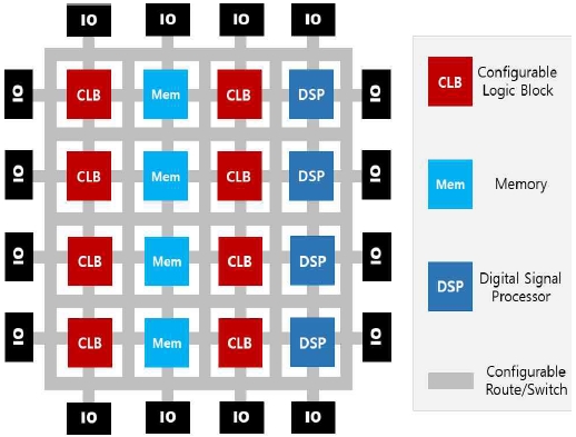
An FPGA is a reconfigurable hardware circuit who’s functionality can be reprogrammed many time. Its performance is better than that of a software but less than ASIC-style implementation of the function. Typically it has been used mainly as a prototyping platform but it is now used as a core part of a System-on-Chip (SoC) for better performance and energy efficiency than pure hardware or software only implementations. Fig. 1 shows a typical internal structure of an FPGA and there are four main components such as configurable logic blocks (CLB), memory, digital signal processor (DSP) and configurable switches and wires [7][11][12]. By programming the CLB and configurable switches/wires, any functional logic circuit can be implemented on the FPGA devices.
2.2 High-Speed Carry Logic in an FPGA
Since an FPGA is a reprogrammable platform with redundant reconfigurable logic blocks, in general, it can not be optimized more than full-custom ASIC-style circuit implementation. In order to overcome such a timing and area performance issue, modern commercial FPGAs adopt dedicated well-optimized dedicated circuits and functional modules such as a digital signal processing (DSP) logic, a block memory and a high-speed carry logic (CARRY4 in an Xilinx FPGA) [10]. Through the uses of such dedicated high-speed IP modules, high performance circuits can be implemented on an FPGA. An addition is a very essential logic component in a modern digital system, so modern FPGA vendors develop an FPGA architecture in which high speed carry propagation paths are implemented as a dedicated logic block in the name of ‘CARRY4’ in Xilinx FPGA devices. Through this dedicated carry propagation path, an adder circuit with a wide bit width can be accelerated.
III. MFC Architecture
3.1 MFC operation and CARRY4 in FPGAs
In a clocking circuit design, a clock frequency can be modulated by adding or subtracting the jitter noise, Δt deviation, to the clock source. Then, the modulated clock can be one of the pre-defined set of small discrete frequencies and the clock changes its frequency over time slightly with intentional jitter. Finally, the power spectrum of the modulated clock will be reduced [6].
The proposed MFC circuit is implemented on an FPGA and it is mainly based on the CARRY4 primitive in the FPGA. We can use carry chains which are available in most FPGA families. The CARRY4 has been designed for implementing adders, accumulators and counters for the digital processing applications. The carry chains which are the dedicated routes between FPGA logic elements have the minimal propagation delay because they are implemented as a hard-macro design. The timing simulation shows the average delay of CARRY4 block in Spartan 6 FPGA is about ‘100 ps’.
In order to utilize the high-speed feature of the CARRY4 block, we utilize the dedicated carry chain structure to generate a finely controllable variable delay line. This is different from the MFC architecture proposed originally in [6] where the delay line is constructed by cascading LUT block resources.
On the otherhand, for obtaining the minimal frequency differences (delay difference) between discrete clock frequencies (1/“clock cycle time”), authors need a high effort to design carefully the relative locations of delay elements as well as the wire delay of their interconnections in the FPGA. Such a low level optimization in an FPGA devices is inefficient and impossible to do in practice.
3.2 Internal Architecture of an MFC
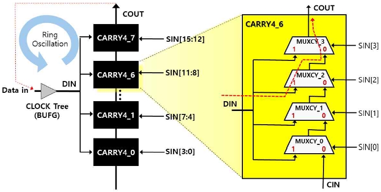
Fig. 2 illustrates the place and routing of CARRY4s chain for an adaptive MFC using eight CARRY4s blocks (from CARRY4_0 to CARRY4_7). Each CARRY4 block provides four builtin multiplexers (MUXCY) and four xor gates (XORCY) [10].
In a single CARRY4 block, we can generate four different delays according to the 4-bit SIN signal. In Fig. 2, the DIN is a single value signal and the signal branches to the input of all the four multiplexers. By properly setting the SIN and DIN signal values, we can make four different carry propagation pattern and it leads to four different delays as follows.
- 1) Shortest Carry Propagation Delay SIN[3:0] = 1111 The incoming DIN signal takes one-MUX delay
- 2) Second Shortest Carry Propagation Delay SIN[3:0] = 0111 The incoming DIN signal takes two-MUX delay
- 3) Third Shortest Carry Propagation Delay SIN[3:0] = 0011 The incoming DIN signal takes three-MUX delay
- 4) Longest Carry Propagation Delay SIN[3:0] = 0001 The incoming DIN signal takes four-MUX delay
In the CARRY4 block presented in the right side of Fig. 2, incoming signal on DIN goes to COUT through MUXCY_2 and MUXCY_3. The propagation path is marked by a dotted line (DIN → MUXCY_2 → MUXCY_3 → COUT). In this case, the SIN[3:0] is set to “0111”.
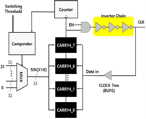
Fig. 3 presents the schematic of the MFC of producing a modulated clock signal (CLK) to a synchronous digital circuit. The eight CARRY4 blocks are serially connected in a form of a chain in order to form a variable delay line.
Together with the CARRY4 chain, an AND gate, a cascaded inverter chain and a global clock tree buffer (BUFG) are connected in a loop to form a closed loop ring (ring oscillator) structure. The proposed ring oscillator is easy to be designed and implemented in an commercial FPGA by using the chain of the odd number inverters (marked by Inverter-Chain in Fig. 3) which are connected in the series. The Inverter- Chain can be implemented by an LUT element on FPGAs if the delay of the chain needs to be large.
Finally the i-th smallest clock cycle time (CCTi) can be described by the following equation, Eq. 1.
| (1) |
Here, DMUXCY is the delay of single MUX element in a CARRY4 block and BCCT is a base clock cycle time which is implemented by configuring the shortest carry propagation length. Note that the DMUXCY is 50 ps in average and the clock cycle time is adjusted at the 100 ps granularity.
Note that In the proposed MFC architecture, the serially cascaded CARRY4 chain has the role as a finely controllable delay element. Based on the ‘32-bit’ SIN signal, a different number of delay is selected as explained before. Each CARRY4s block has four delay elements. Thus, an “eight-CARRY4s” generate totally thirty two (4 ✕ 8 = 32) different delays which are corresponding to thirty two different clock frequencies.
On the other hand, in order to guarantee the feedback CLK (marked by “Data in” Fig. 3) arriving to the eight CARRYs at the same time, we use the global clock tree line (BUFG) in the design. The BUFG is a FPGA dedicated resource and it has a role of amplifying signal strength so the “Data in” signal propagates to the input of the CARRY4 blocks in a high speed. That means the arrival time of the “Data in” signal at the eight CARRY4 blocks are almost similar to each other.
The counter and comparator are used for the MUXs to select one of incoming value for 32-bit SIN signal. The output of the MUX becomes an input to the eight CARRY4s. The switching threshold value is defined as the number of clock cycles and during the number of clock cycles, selected clock frequency is utilized to drive a synchronous digital system. After consuming the number of clock cycles, new clock frequency is selected. Actually, it is the parameter to select the modulation frequency of the proposed MFC design.
In our design, the switching frequency defines the rate at which the operating frequency is changed. The bit width of the counter is calculated based on the switching frequency and the operating frequency:
| (2) |
In Eq. 2, m is a number of bits in a counter, fo is an operating frequency and fsw is a switching frequency. To ensure the input values of the SIN for each CARRY4 block become stable before the “Data in” arrives, the following timing constraint needs to be satisfied:
| (3) |
In Eq. 3, Tcounter, Tcomp and TMUX are the delay of a counter, a comparator and a multiplexer, respectively. TAND, Tinverter-chain and TBUFG are the delay of an AND gate, an inverter chain and a BUFG, respectively. By controlling Tinverter-chain, we can make the constraint be satisfied for correct operations.
Ⅳ. Experimental Results
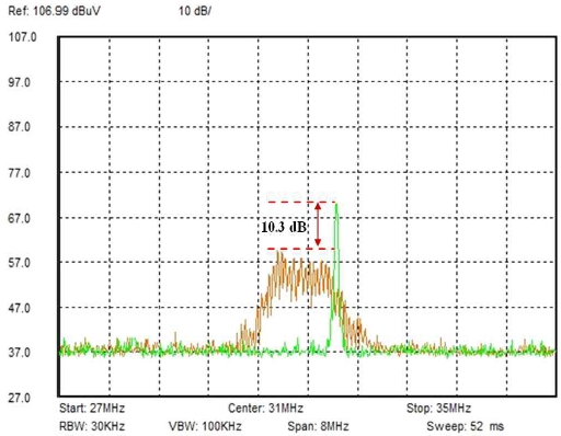
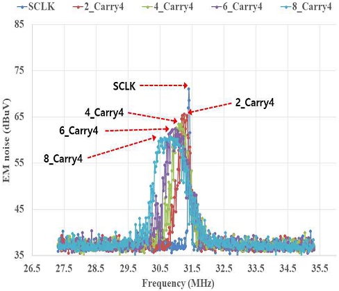
Our proposed architecture has been implemented on the development board employing a Xilinx Spartan-6 FPGA. The EMI measurement results are shown in Fig. 3 and Fig. 4.
For the measurement, we use a spectrum analyzer. In the case of using eight CARRY4s, the highest reduction of peak power is about 10.41dB compared to the single clock frequency as shown in Fig. 4.
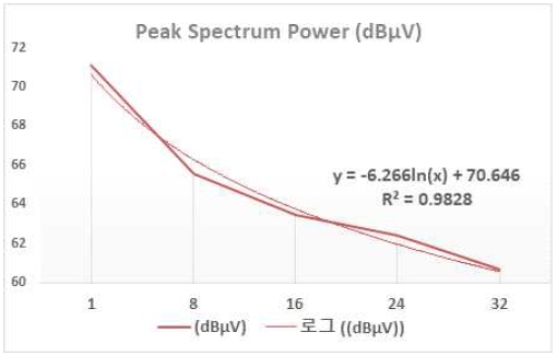
Table 1 show the maximum spectrum powers measured from experiments for single clock system, 8-freq., 16-freq., 24-freq. and 32 freq. in MFC systems.
As presented in Table 1, we observed the highest EMI reduction, about 10.41dB, when using eight CARRY4 blocks (employing 32 clock frequencies for spreading spectrum power). The reason is that the spreading range of the eight CARRY4s is wider than those of three other cases.
V. Tradeoff Analysis
As we increase the number of clock frequencies for modulation, we can obtain more EMI reduction as shown in
Table 1, we lost some performance. In order to perform tradeoff analysis, we approximate the peak power reduction trend with a log function as shown in Fig. 6. Then, the approximated function for peak spectrum power is fitted with R2 = 0.98 as the following equation (Eq. 4).
| (4) |
The average of increased clock cycle time is about `100 ps` in average (it means that clock frequency is reduced proportionally as the cycle time increases) when we increase carry chain length one more as shown in Eq. 1.
The average clock cycle time () of employing ‘n’ clock frequencies can be described by the following equation, Eq. 5.
| (5) |
Finally, the performance overhead (Overhead) caused by employing multiple clock frequencies can be presented by the following equation. Eq.6.
| (6) |
Table 2 shows estimated performance overhead according to Eq. 6. For the estimation, ‘31.84 ns’ is used for BCCT since we used the clock frequency, 31.4 MHz, for the minimum clock frequency of the MFC in experiments. Then, `50 ps` is used for ‘DMUXCY’.
As shown in Table 2, the performance overhead is less than 5%. However, in some system, such a performance loss can be critical problem. It will be a designer’s choice for selecting most suitable number of frequencies in the MFC for the target application system depending on the EMI regulation.
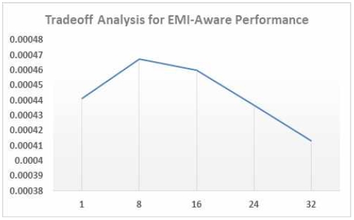
Finally, a new metric, EMI-awared performance, for tradeoff analysis can be formulated as a product of 1/EMIApprox and 1/CCTnAvg in the following equation.
| (7) |
Fig. 7 shows the EMI-aware performance for an MFC system. When we consider both of peak EM noise and performance, the use of “8 clock frequencies” will be best choice. Nevertheless, the proper choice for the number of clock frequencies in MFC has to be considered together with EMI regulation since satisfying the regulation is higher priority then performance in some safety critical system design.
Ⅵ. Conclusion
This paper proposed a new MFC architecture based on a high-speed dedicated FPGA resource called a CARRY4 block. Then, we evaluated an EMI reduction of the MFC circuit utilizing the carry chains in FPGA. Our proposed architecture was implemented on a Spartan-6 FPGA based board and it had the advantages of low cost and easy implementation on an FPGA thanks to the fully digitalized structure when compared to the design of the conventional spread spectrum generator. However, performance overhead increases as the number of frequencies increases in an MFC design, so that system designers need to do tradeoff analysis for optimal target system design.
Acknowledgments
This work was supported by the Hallym University Research Fund (grant number H20180095)
References
-
M. Ramdani, et al, "The electromagnetic compati-bility of integrated circuits: Past, present and future", IEEE Trans. Electromagn. Compat., Vol. 51, No. 1, pp. 78-100, Feb. 2009.
[https://doi.org/10.1109/TEMC.2008.2008907]

-
M. H. Oh, H. Y. Kim, and J. G. Lee, "Analysis on Low-Voltage Operation Behavior and EMI Emission in Asynchronous Processor", The Journal of KIIT, Vol. 12, No. 2, pp. 33-40, Feb. 2014.
[https://doi.org/10.14801/kiitr.2014.12.2.33]

-
F. Fiori and M. Merlin, "A new grounding scheme to reduce the electromagnetic emission of smart-power system-on-chips", IEEE Trans. Power Electron., Vol. 27, No. 1, pp. 224–234, Jan. 2012.
[https://doi.org/10.1109/TPEL.2010.2068312]

-
H. Fujita, et al, "Evaluation of PDN impedance and power supply noise for different on-chip decoupling structures", in Proc. 9th Int. Workshop Electromagn. Compat. Integr. Circuits (EMC Compo), Nara, Japan, pp. 142–146, Dec. 2013.
[https://doi.org/10.1109/EMCCompo.2013.6735189]

-
M. Badaroglu, et al, "Digital Ground Bounce Reduction by Supply Current Shaping and Clock Frequency Modulation", IEEE Trans. Computer Aided Design, Vol. 24, No. 1, pp. 65 -76, Jan. 2005.
[https://doi.org/10.1109/TCAD.2004.839471]

-
J. G. Lee, "A Low EMI Circuit Design with Asynchronous Multi Frequency Clocking", IEICE Transaction Electron, Vol. E97-C No. 12, pp. 1158-1161, Dec. 2014.
[https://doi.org/10.1587/transele.E97.C.1158]

- P. Y. Wang and S. P. Chen, "Spread spectrum clock generator", IEEE Asian Solid-State Circuits Conference, Nov. 2007.
-
W. Y. Lee and L. S. Kim, "A Spread Spectrum Clock Generator for DisplayPort", IEEE Trans. Circuits Syst, II, Exp. Briefs, Vol. 58, No. 6, pp. 361-365, Jun. 2011.
[https://doi.org/10.1109/TCSII.2011.2149670]

-
S. G. Bae, G. Kim, and C. Kim, "A 5-GHz subsampling PLL-based spread-spectrum clock generator by calibrating the frequency deviation", IEEE Trans. Circuits Syst. II, Exp. Briefs, Vol. 64, No. 10, pp. 1132-1136, Oct. 2017
[https://doi.org/10.1109/TCSII.2016.2624759]

- Xilinx, "7 Series FPGAs Configurable Logic Block: User Guide", Sep. 2016.
-
D. Y. Lee and J. G. Lee, "Design Space Exploration and Analysis for Electromagnetic Emission in a Digital FPGA Chip", The Journal of KIIT, Vol. 14, No. 8, pp. 11-19, Aug. 2016.
[https://doi.org/10.14801/jkiit.2016.14.8.11]

- N. V. Toan, et al, "Design of a multi-frequency clocking circuit on an FPGA and analysis of its EMI emission", Asia-Pacific Symposium on Electromagnetic Compatibility (APEMC), Shenzhen, China, pp. 598-600, May 2016.

Feb. 1996: Dept. of Computer Science, Hallym University (BS)
Feb. 1998: Dept. of Info. and Comm., Gwangju Institute of Science and Techology (ME)
Feb. 2005: Dept. of Info. & Comm., Gwangju Institute of Science & Techology (Ph.D)
Feb. 2008 ~ present : Professor, School of Software, Hallym University
Research topic : Digital Integrated Circuit, Asynchronous Circuit, Electromagnetic Interference.

Feb. 1993 : Dept. of Computer Science, Kangwon National University (BS)
Feb. 1999 : Dept. of Computer Science, Kangwon National University (MS)
Aug. 2006 : Dept. of Computer Science, Kangwon National University (Ph.D)
Sep. 2003 ~ present : Assistant professor, College of General Education, Hallym University
Research topic : Arithmetic Circuit, Computer Architecture, Computer Programming Education

